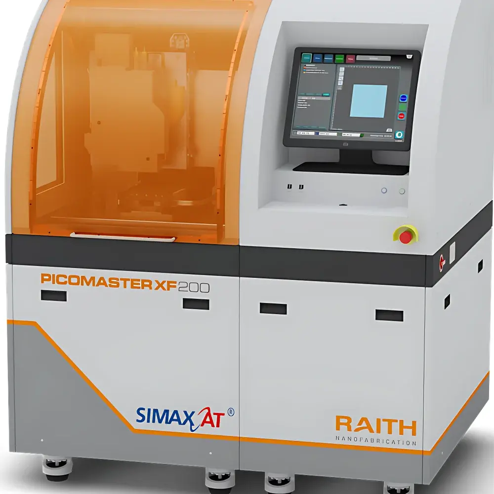
Raith PicoMaster XF ATE-200 Direct Write Lithography System
| Brand | Raith / Simax |
|---|---|
| Origin | Netherlands |
| Manufacturer Type | Authorized Distributor |
| Import Status | Imported |
| Model | PicoMaster XF ATE-200 |
| Exposure Mode | Proximity Mode |
| Resolution | 600 nm |
| Light Source | GaN Laser Diode |
| Wavelength | 405 nm |
| Illumination Uniformity | ±5% |
| Maximum Exposure Area | 200 mm × 200 mm |
| Maximum Write Speed | 280 mm²/min |
| Minimum Feature Size | 600 nm |
Overview
The Raith PicoMaster XF ATE-200 is a high-precision, benchtop direct write lithography system engineered for rapid prototyping and low-volume fabrication of microstructures in academic research labs, semiconductor process development centers, and MEMS/NEMS pilot lines. Unlike mask-based photolithography tools, this system employs a focused 405 nm gallium nitride (GaN) laser diode beam scanned via high-speed galvanometric mirrors to directly pattern photoresist-coated substrates without physical masks. Its proximity-mode exposure architecture enables uniform energy delivery across large fields while maintaining sub-micron feature fidelity—ideal for applications where design iteration speed, mask cost avoidance, and process flexibility outweigh the throughput requirements of full-wafer steppers. The system operates on standard optical tables and integrates seamlessly into cleanroom environments classified ISO Class 5 or better.
Key Features
- Proximity-mode exposure architecture with calibrated gap control (10–50 µm adjustable) for consistent dose transfer and minimized diffraction effects
- 405 nm GaN laser source delivering stable output power (>50 mW) with <±0.5% intensity drift over 8-hour operation
- High-resolution beam positioning enabled by dual-axis galvo scanners with closed-loop feedback and <100 nm positional repeatability
- 200 mm × 200 mm maximum exposure field—compatible with 4-inch wafers, glass slides, silicon substrates, and flexible polymer foils
- Real-time dose modulation via analog laser current control, supporting grayscale lithography and multi-dose layer alignment
- Integrated environmental monitoring (temperature, humidity, vibration) with automated compensation routines for long-exposure stability
- Modular vacuum chuck system with programmable clamping pressure and optional backside helium cooling for thermal management during extended writes
Sample Compatibility & Compliance
The PicoMaster XF ATE-200 accommodates substrates ranging from 10 mm × 10 mm up to 200 mm × 200 mm, including silicon, fused silica, sapphire, ITO-coated glass, and polyimide films. Substrate thickness tolerance spans 0.1 mm to 5 mm, with automatic Z-height mapping and focus correction. Resist compatibility covers standard positive (e.g., AZ® 1518, PMMA 950K), negative (SU-8 2000 series), and high-resolution chemically amplified resists (CARs). The system conforms to CE marking requirements and meets electromagnetic compatibility standards per EN 61326-1. All motion control firmware and laser drivers comply with IEC 61508 SIL2 for functional safety in lab automation environments. Documentation packages support GLP-compliant audit trails when used with optional Raith LogBook software.
Software & Data Management
Control is executed through Raith’s proprietary Nanosuite™ v6.x platform—a Windows-based application supporting GDSII, OASIS, DXF, and SVG import with real-time polygon decomposition and hierarchical flattening. Pattern generation includes proximity effect correction (PEC) using built-in kernel convolution models, dose matrix optimization, and stitching error compensation across adjacent fields. Data logging captures timestamped exposure parameters (laser power, scan velocity, stage position, ambient conditions), stored in HDF5 format for traceability. Optional integration with LabArchives ELN or Thermo Fisher SampleManager enables metadata synchronization and CFR Part 11–compliant electronic signatures when configured with hardware security modules (HSMs).
Applications
- Rapid prototyping of photonic crystals, plasmonic metasurfaces, and diffractive optical elements (DOEs)
- Fabrication of microfluidic channel networks, lab-on-chip devices, and electrochemical sensor electrodes
- Development of MEMS accelerometers, RF resonators, and piezoelectric transducers requiring sub-µm alignment tolerances
- Maskless fabrication of quantum device test structures (e.g., superconducting qubit arrays, spin qubit gates)
- Education and training in nanofabrication workflows—enabling students to execute full design-to-pattern cycles within a single lab session
- Hybrid lithography: combining PicoMaster-written alignment marks with subsequent e-beam or nanoimprint steps
FAQ
Does the PicoMaster XF ATE-200 support electron-beam resist processing?
Yes—it is fully compatible with standard e-beam resists such as PMMA, HSQ, and ZEP, though exposure is performed optically at 405 nm; resist sensitivity must be verified empirically for each formulation.
Can it perform multi-layer alignment with sub-micron accuracy?
Yes—using integrated CCD-based alignment cameras and fiducial recognition algorithms, overlay accuracy of ≤±150 nm (3σ) is achievable between layers.
Is vacuum required for operation?
No vacuum chamber is needed; however, optional vacuum chucking is available for substrate immobilization during high-speed scanning.
What maintenance intervals are recommended for the laser source?
The GaN laser diode has a rated lifetime of >10,000 hours; annual intensity calibration and collimation verification are advised per Raith Service Protocol RP-XF-02.
Is remote operation supported for shared facility use?
Yes—via secure RDP or VNC connections with role-based access control; network configuration adheres to IEEE 802.1X authentication standards.


