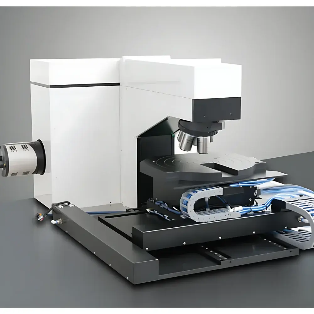
RAMANdrive Raman Microscope by Bruker
| Brand | Bruker |
|---|---|
| Origin | Germany |
| Manufacturer Type | Authorized Distributor |
| Origin Category | Imported Instrument |
| Model | Nanophoton RAMANdrive |
| Instrument Type | Fourier Transform Raman Spectrometer |
| Spatial Resolution | 350 nm (X), 500 nm (Y), 1 µm (Z) |
Overview
The RAMANdrive Raman Microscope by Bruker is an advanced, high-throughput confocal Raman imaging system engineered for precision chemical mapping and structural characterization at sub-micron spatial resolution. Unlike conventional point-scanning Raman microscopes that rely on mechanical stage movement, the RAMANdrive employs patented galvanometric mirror-based line-scan technology developed by Nanophoton. This architecture decouples laser beam positioning from physical sample translation—enabling rapid, vibration-free spectral acquisition across large fields of view. The system operates on a Fourier Transform Raman principle optimized for low-fluorescence, high-stability measurements, with integrated notch filtering, high-quantum-efficiency CCD detection, and thermoelectric cooling to ensure signal fidelity. Designed specifically for semiconductor process control and failure analysis, it delivers quantitative molecular contrast without destructive labeling or vacuum requirements—making it ideal for in-line metrology and R&D environments where speed, reproducibility, and traceable calibration are critical.
Key Features
- Galvo-driven line-scan excitation: Eliminates stage-induced mechanical drift and microvibrations, enabling stable acquisition over extended measurement durations.
- Sub-diffraction spatial resolution: Achieves 350 nm lateral resolution in X, 500 nm in Y, and 1 µm axial (Z) resolution—validated per ISO 18564-1 for Raman microscopy performance reporting.
- High-throughput spectral acquisition: Captures up to 400 full Raman spectra simultaneously in on-line spot mode, significantly reducing total imaging time versus raster-scan equivalents.
- Dedicated 300 mm (12-inch) wafer stage: Fully motorized, vacuum-compatible platform with programmable Z-height compensation for flatness-critical semiconductor substrates.
- AreaFlash™ averaging mode: Acquires multiple line scans across user-defined regions and computes pixel-wise spectral averages in real time—enhancing signal-to-noise ratio without increasing dwell time.
- Cleanroom-compatible design: Compliant with ISO Class 5 environmental specifications; includes ESD-safe housing, particle-shielded optics, and non-outgassing materials.
Sample Compatibility & Compliance
The RAMANdrive supports a broad range of solid-state and thin-film samples including silicon wafers, compound semiconductors (GaN, SiC), 2D materials (graphene, TMDCs), polymer resists, and dielectric stacks. Its non-contact, non-destructive nature ensures integrity preservation during repeated inspection cycles. System compliance includes adherence to IEC 61000-6-3 (EMC emissions), IEC 61000-6-2 (immunity), and alignment with ASTM E1840 and ISO/IEC 17025 documentation requirements for analytical instrument qualification. Optional IQ/OQ protocols support GMP/GLP-regulated laboratories, while audit trail functionality meets FDA 21 CFR Part 11 criteria when paired with Bruker’s OPUS software suite.
Software & Data Management
Controlled via Bruker’s OPUS 8.x platform, the RAMANdrive integrates native support for hyperspectral data cubes (FITS and HDF5 formats), multivariate analysis (PCA, cluster analysis), and automated phase identification using the commercial RRUFF and ICDD Raman databases. Real-time spectral preprocessing includes cosmic ray removal, baseline correction (Asymmetric Least Squares), and intensity normalization. Data export conforms to ASTM E131 and ISO 14644-1 metadata standards. Secure user role management, electronic signatures, and full audit logging—including parameter changes, acquisition timestamps, and detector gain settings—are enabled by default for regulated workflows.
Applications
- Semiconductor metrology: Strain mapping in FinFET structures, dopant distribution profiling, gate oxide thickness verification, and interfacial reaction layer identification.
- Failure analysis: Correlation of Raman shifts with thermal stress, crystallinity loss, or defect density in packaged ICs and 3D NAND stacks.
- Materials science: Phase segregation analysis in perovskite solar cells, grain boundary chemistry in polycrystalline films, and interlayer coupling in van der Waals heterostructures.
- Quality assurance: Batch-to-batch consistency checks for photoresist composition, CMP slurry residue detection, and contamination screening on reticles and masks.
- Process integration: Direct interfacing with automated defect review stations (e.g., KLA eDR72xx series) via SECS/GEM protocol for closed-loop feedback in fab environments.
FAQ
Is the RAMANdrive compatible with existing cleanroom automation infrastructure?
Yes—the system supports standard SEMI E30 (GEM) and E40 (SECS-II) communication protocols, enabling seamless integration into 300 mm fab AMHS and MES systems.
Does the system require external water cooling or compressed air?
No—all thermal management is handled internally via closed-loop thermoelectric coolers and passive heat sinks, eliminating utility dependencies beyond standard 230 VAC power.
Can spectral calibration be performed in situ without removing optics?
Yes—integrated neon and silicon reference sources allow fully automated wavelength and intensity calibration before each session, traceable to NIST SRM 2241.
What is the maximum usable field of view for single-acquisition mapping on a 12-inch wafer?
With the optional wide-field objective and AreaFlash™ mode, up to 10 × 10 mm² can be mapped at 1 µm/pixel resolution in under 12 minutes, maintaining <±0.1 cm⁻¹ wavenumber accuracy across the entire area.
How is data integrity ensured during long-duration acquisitions?
OPUS implements cyclic redundancy checksums for every acquired spectrum, automatic file versioning, and SHA-256 hash generation for raw data packages—ensuring forensic-level traceability per ISO/IEC 17025 clause 7.5.2.