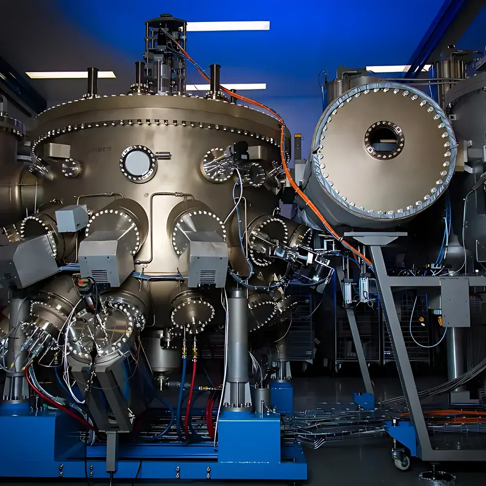
RIBER MBE 8000 Molecular Beam Epitaxy System
| Brand | RIBER |
|---|---|
| Origin | France |
| Model | MBE 8000 |
| Substrate Size | 8×6″ or 4×8″ |
| Base Vacuum | ≤1.0×10⁻¹⁰ Torr |
| Thickness Uniformity (InGaAs/GaAs SL on 8×6″ platen) | ±1.5% |
| Composition Uniformity (InGaAs/GaAs SL) | ±1.5% |
| AlAs/GaAs SL Thickness Uniformity | ±1.5% |
| Si Doping Standard Deviation Uniformity | <3% |
| Fabry–Perot Dip Wavelength Uniformity (8×6″ wafer) | Δλ < 3 nm |
| Background Carrier Density | 7×10¹⁴ cm⁻³ |
| HEMT Electron Mobility @ RT | 6000 cm²·V⁻¹·s⁻¹ |
| HEMT Electron Mobility @ 77 K | 120,000 cm²·V⁻¹·s⁻¹ |
| GaN-based HEMT Mobility @ 77 K | 178,000 cm²·V⁻¹·s⁻¹ |
| InGaAs/GaAs Superlattice Thickness | 298 Å ± 2 Å |
Overview
The RIBER MBE 8000 is a high-precision molecular beam epitaxy system engineered for the controlled growth of atomically ordered epitaxial thin films under ultra-high vacuum (UHV) conditions. Operating at base pressures ≤1.0×10⁻¹⁰ Torr, the system enables stoichiometrically precise, layer-by-layer deposition via thermal effusion from multiple solid-source Knudsen cells. Its core architecture integrates a UHV-compatible main chamber with differential pumping stages, a multi-axis substrate manipulator (including rotation, tilt, and vertical translation), and a high-stability substrate heater capable of uniform temperature distribution up to 1100 °C. The MBE 8000 implements real-time in-situ monitoring via reflection high-energy electron diffraction (RHEED), enabling atomic-scale feedback during growth initiation, interface formation, and superlattice periodicity control. Designed for research-grade epitaxy of III–V, II–VI, IV–IV, and emerging wide-bandgap semiconductors—including GaAs, InP, GaN, SiGe, and complex heterostructures—the system supports fundamental studies of surface kinetics, interfacial thermodynamics, and quantum confinement effects.
Key Features
- Modular UHV chamber architecture with all-metal sealing and bake-out capability to 200 °C, ensuring long-term vacuum integrity and low hydrocarbon background.
- Up to 12 independently controlled effusion cells with high-resolution shutter actuation (≤10 ms response time) and integrated flux calibration via quartz crystal microbalances (QCMs) and RHEED intensity oscillation analysis.
- Dual-mode substrate heating: resistive heating for precise temperature ramping (±0.5 °C stability) and electron-beam-assisted heating for localized thermal management during growth interruption or annealing.
- Automated sample transfer system with load-lock and cryo-pumped transfer chamber, supporting batch processing of up to 25 wafers per run without breaking main chamber vacuum.
- Integrated RHEED system with phosphor-screen imaging and digital CCD acquisition, synchronized with shutter timing for real-time growth rate and surface reconstruction monitoring.
- Full I/O compatibility with LabVIEW-based control software, supporting programmable growth recipes with conditional logic, data logging at ≥10 Hz sampling rate, and hardware-triggered event capture.
Sample Compatibility & Compliance
The MBE 8000 accommodates substrates up to 8×6″ (203×152 mm) or 4×8″ (102×203 mm) formats—compatible with standard semiconductor wafer carriers and custom holders for non-planar or patterned substrates. It supports native oxide removal via in-situ atomic hydrogen cleaning and thermal desorption prior to nucleation. All wetted materials comply with ASTM F1318 (Standard Specification for High-Purity Metals for Semiconductor Applications) and ISO 14644-1 Class 4 cleanroom handling protocols. The system’s vacuum design meets EN 61000-6-3 (EMC emission limits) and EN 61000-6-2 (immunity requirements). For regulated environments, optional audit-trail-enabled software modules support 21 CFR Part 11 compliance, including electronic signatures, user role-based access control, and immutable raw data archiving.
Software & Data Management
The RIBER MBE Control Suite provides deterministic, deterministic real-time process orchestration through a deterministic real-time OS kernel. Growth recipes are defined in hierarchical XML schema, supporting nested subroutines, parameter interpolation, and inter-step dependency validation. All sensor inputs—including cell temperatures, shutter states, RHEED intensities, QCM rates, and substrate thermocouple readings—are timestamped with nanosecond precision and stored in HDF5 format for post-growth analysis. Built-in spectral analysis tools enable FFT-based oscillation frequency extraction from RHEED traces, while thickness calibration models incorporate flux divergence correction and shadowing compensation. Export modules generate standardized reports compliant with ISO/IEC 17025 documentation requirements, including uncertainty budgets for thickness and composition values.
Applications
- Growth of lattice-matched and strained heterostructures for high-electron-mobility transistors (HEMTs), with demonstrated reproducibility in AlGaN/GaN and InAlAs/InGaAs channel layers.
- Atomic-layer engineering of quantum wells, dots, and wires for mid-IR photodetectors, quantum cascade lasers, and single-photon emitters.
- Epitaxial development of topological insulator thin films (e.g., Bi₂Se₃, Sb₂Te₃) and 2D van der Waals heterostructures requiring atomically sharp interfaces.
- Fundamental investigation of surfactant-mediated growth kinetics, step-flow vs. layer-by-layer transition thresholds, and dopant incorporation profiles using secondary ion mass spectrometry (SIMS)-correlated samples.
- Process qualification for compound semiconductor foundry pilot lines, where thickness uniformity <±1.5% and compositional variation <±1.5% across 8×6″ wafers meet industry benchmarking criteria for device yield prediction.
FAQ
What vacuum level is required for stable MBE operation, and how is it maintained?
The MBE 8000 achieves and sustains a base pressure ≤1.0×10⁻¹⁰ Torr using a combination of turbomolecular pumps with cryogenic backing, ion pumps, and titanium sublimation pumps—all integrated into a differential pumping architecture that isolates source zones from the growth zone.
Can the system grow nitride-based materials such as GaN or AlN?
Yes—the chamber is fully compatible with active nitrogen cracking sources (RF or ECR plasma), and the substrate heater supports the high temperatures (>750 °C) and precise N/Ga flux ratios required for stoichiometric GaN growth.
Is remote operation and monitoring supported?
The system includes secure TLS-encrypted remote access via Ethernet, enabling real-time dashboard viewing, recipe upload/download, and emergency shutdown from off-site locations—fully auditable under GLP/GMP workflows.
How is film thickness calibrated and verified in situ?
Thickness is calibrated using both RHEED intensity oscillation period analysis and quartz crystal microbalance (QCM) deposition rate cross-validation; final verification is performed via ex-situ X-ray reflectivity (XRR) and high-resolution transmission electron microscopy (HRTEM) correlation.
Does the system support automated growth interruption and annealing sequences?
Yes—programmable growth pauses with simultaneous substrate cooling/heating, shutter sequencing, and ambient gas introduction (e.g., As₂ or PH₃) are fully scriptable within the control suite, enabling controlled interface reconstruction and defect passivation steps.


