RKD RA-880 Laser Chip Decapsulation System
| Brand | RKD |
|---|---|
| Origin | USA |
| Model | RA-880 Laser Decapsulation System |
| Application | Semiconductor Plastic Encapsulant Removal |
| Compliance | Designed for ISO/IEC 17025-aligned failure analysis labs |
| Software Control | Windows-based real-time co-focal imaging & programmable laser scanning platform |
| Laser Type | Q-switched Nd:YAG (1064 nm) with variable pulse width and energy modulation |
| Focus Control | Auto-focus sensor with programmable depth-of-field (DOF) adjustment |
| Imaging | Integrated high-resolution coaxial CCD with 10×–50× optical zoom and real-time overlay of scan path |
| Pattern Definition | Vector-based graphical interface supporting DXF, JPEG, BMP import |
| Energy Management | Closed-loop pulse energy monitoring with ±2% stability |
| Reproducibility | <±3 µm positional repeatability across >1000 cycles |
| Maintenance | Solid-state laser source |
Overview
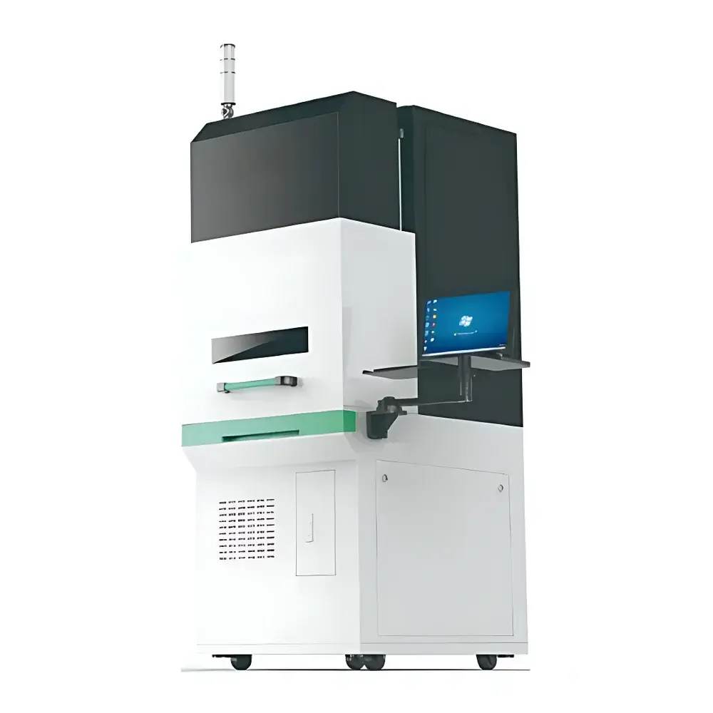
The RKD RA-880 Laser Chip Decapsulation System is an engineered solution for non-destructive, precision removal of plastic encapsulants from semiconductor devices. It employs a Q-switched Nd:YAG laser operating at 1064 nm wavelength, delivering controlled thermal ablation through pulsed photothermal interaction—minimizing substrate heating while selectively volatilizing epoxy molding compounds (EMCs), silicone gels, and other organic encapsulants. Unlike wet chemical decapsulation (e.g., fuming nitric or sulfuric acid), the RA-880 eliminates hazardous reagent handling, reduces process variability, and preserves bond wires (Au, Cu, Al, Ag), die attach materials, and underlying metallization. Its co-focal imaging architecture synchronizes real-time video capture with laser scanning coordinates, enabling sub-50 µm feature resolution and traceable process documentation—critical for root cause analysis in high-reliability applications including automotive AEC-Q100, aerospace DO-254, and medical ISO 13485 environments.
Key Features
- Real-time co-focal imaging system with coaxial high-magnification optics (10×–50× zoom) and live overlay of laser scan path on captured video feed
- Auto-focus sensor with programmable focal plane tracking and depth-of-field control—enabling consistent ablation across stepped topographies (e.g., stacked dies, molded interconnect devices)
- Vector-based pattern editor supporting import of X-ray, C-SAM, SEM, and optical microscopy images (JPEG, BMP, DXF); allows precise alignment of ablation zones to internal defects or bond wire locations
- Energy-regulated pulse delivery with closed-loop monitoring—ensuring ±2% pulse-to-pulse energy stability for repeatable material removal without charring or microcracking
- Programmable recipe storage for up to 500 decapsulation protocols—including layer-specific power/dwell settings, multi-step depth profiling, and secondary bond pad exposure sequences
- No consumables required; solid-state laser source rated for >12,000 operational hours; maintenance intervals aligned with ISO/IEC 17025 calibration schedules
Sample Compatibility & Compliance
The RA-880 accommodates standard JEDEC trays, waffle packs, and individual DIP, SOIC, QFP, QFN, BGA, and discrete packages (TO-220, SOT-23). It supports decapsulation of leadframe-based plastic ICs, molded discrete diodes/transistors, and advanced packaging formats including flip-chip-on-PCB and flip-chip-on-ceramic substrates. The system meets IEC 60825-1:2014 Class 4 laser safety requirements and integrates interlocked enclosure with visible/IR beam shutters. Process outputs are fully traceable per FDA 21 CFR Part 11 (with optional electronic signature module) and support GLP/GMP audit trails for regulated failure analysis workflows. All ablation parameters—including laser fluence (J/cm²), pulse count, dwell time, and XY coordinate logs—are timestamped and exportable in CSV/JSON format.
Software & Data Management
Controlled via a dedicated Windows 10 IoT Enterprise platform, the RA-880 software provides full GUI-driven operation with dual-display capability: one screen for real-time imaging and overlay, the other for parameter configuration and historical recipe recall. The system implements AES-256 encrypted local database storage for all session logs, image captures, and operator actions. Export options include annotated TIFF stacks, measurement-embedded PDF reports, and XML-formatted process metadata compatible with LIMS integration (e.g., Thermo Fisher SampleManager, LabVantage). Audit trail functionality records user ID, timestamp, parameter changes, and emergency stop events—meeting ISO/IEC 17025 clause 7.9 and ASTM E2911-22 requirements for analytical instrument data integrity.
Applications
- Precise pre-decap trenching for power semiconductor modules prior to cross-sectioning or acoustic microscopy
- Localized exposure of bond wires and die surfaces for post-failure electrical testing (e.g., probe station validation)
- Removal of top mold compound in flip-chip assemblies to enable underfill inspection or solder joint assessment
- Preparation of TEM/SEM cross-section specimens with minimal mechanical damage or thermal artifact
- Targeted ablation of conformal coatings (e.g., parylene, silicone) for selective defect access in hermeticity-tested devices
- Micro-cutting of metal traces on PCB substrates for isolation of circuit blocks during debug analysis
- Depth-resolved decapsulation for multi-layer stacked-die packages (e.g., 3D NAND, SiP modules)
FAQ
Does the RA-880 require acid or other chemical agents during operation?
No. The system performs entirely dry, laser-based ablation—eliminating reliance on nitric, sulfuric, or phosphoric acid baths.
Can it decapsulate copper wire-bonded devices without damaging the bonds?
Yes. Pulse energy and dwell time are calibrated to remove EMC while maintaining thermal budgets below copper oxidation thresholds (≤200°C peak localized temperature).
Is the system compatible with failure analysis lab information management systems (LIMS)?
Yes. Structured data export (CSV, XML) and API-ready metadata fields support integration with major LIMS platforms per ASTM E2911-22 Annex A2.
What is the typical ablation rate for standard 1.5 mm thick EMC?
Approximately 15–25 µm per pulse at optimal fluence; total decap time for a 5 mm × 5 mm area ranges from 4–12 minutes depending on layer thickness and composition.
Does the RA-880 support automated batch processing of multiple devices?
Yes—via programmable stage movement and barcode-triggered recipe loading; compatible with robotic wafer handlers using RS-232/Modbus TCP interfaces.


