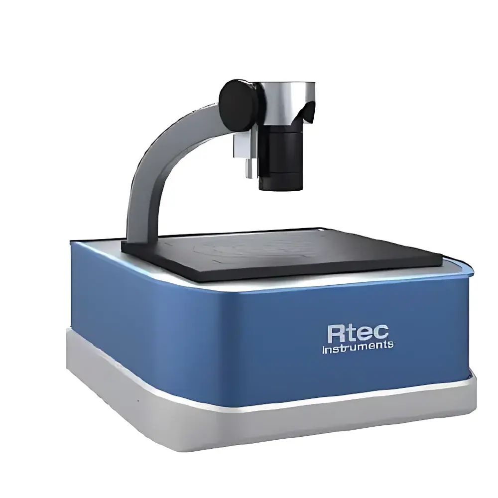
Rtec FT-100 White Light Interferometric Thin-Film Thickness Measurement System
| Brand | Rtec |
|---|---|
| Origin | Switzerland |
| Model | FT-100 |
| Thickness Range | 1 nm – 1.8 mm |
| Wavelength Range | 200 nm – 1700 nm |
| Precision | <0.01 nm or 0.01% |
| Stability | <0.02 nm or 0.03% |
| Spot Size | 4 µm – 200 µm (optional 2 mm field) |
| Measurement Capabilities | Single/multilayer thickness, refractive index (n), extinction coefficient (k), reflectance, transmittance |
| Sample Compatibility | Transparent, semi-transparent, low-absorption films—including liquid films and air-gap layers |
| Platform Integration | Compatible with XY motorized stages for full-sample thickness mapping |
Overview
The Rtec FT-100 is a high-precision white light interferometric (WLI) thin-film thickness measurement system engineered for non-contact, label-free characterization of optical thin films across research laboratories, semiconductor process development, and advanced coating QA/QC environments. Operating on the principle of spectral-domain white light interferometry, the FT-100 analyzes interference fringes generated by broadband light reflected from multiple interfaces within a film stack—enabling simultaneous extraction of physical thickness, complex refractive index (n + ik), and spectral reflectance/transmittance data. Unlike ellipsometry or stylus profilometry, WLI provides intrinsic depth resolution without angular constraints or mechanical contact, making it uniquely suited for fragile, soft, or volatile films—including aqueous layers, polymer resists, and vacuum-deposited dielectrics. Its extended spectral coverage (200–1700 nm) supports both UV-curable coatings and near-infrared photonic structures, while sub-angstrom stability ensures traceable repeatability under ambient lab conditions.
Key Features
- Sub-nanometer thickness resolution: Achieves <0.01 nm absolute precision or 0.01% relative accuracy—validated against NIST-traceable SiO₂/Si reference standards.
- Multi-parameter optical modeling: Integrated inversion algorithm solves for thickness, n(λ), k(λ), and interfacial roughness in single- and multilayer stacks (up to 10 layers) using least-squares fitting of measured spectra.
- Variable spot size optics: Interchangeable objectives support spatially resolved measurements from 4 µm (for micro-patterned devices) to 200 µm (for macro-scale uniformity assessment); wide-field 2 mm mode enables rapid area screening.
- Non-destructive, ambient-environment operation: No vacuum, sputtering, or conductive coating required—ideal for organic electronics, biological membranes, and hygroscopic materials.
- Modular hardware architecture: Designed for OEM integration—optical head mounts directly onto Rtec’s MX series nano-mechanical test platforms, including 3D confocal profilometers, nanoindenter modules, and reciprocating tribometers.
Sample Compatibility & Compliance
The FT-100 accommodates planar and gently curved substrates (radius ≥5 mm) with surface roughness <50 nm RMS. It characterizes films deposited on silicon, fused silica, sapphire, glass, PET, and metal oxides—regardless of substrate opacity—by analyzing spectral interference exclusively from the film-substrate and air-film interfaces. Liquid films (e.g., Langmuir-Blodgett monolayers, spin-coated sol-gels) and nanoscale air gaps (e.g., MEMS cavity spacers) are routinely measured using environmental chamber options. All firmware and calibration routines comply with ISO/IEC 17025 metrological traceability requirements. Data acquisition workflows support audit-ready documentation per FDA 21 CFR Part 11 when deployed in GMP-regulated settings—featuring electronic signatures, version-controlled method files, and immutable raw-data archiving.
Software & Data Management
Control and analysis are performed via Rtec’s proprietary FilmScan™ software (v5.2+), built on a deterministic real-time acquisition engine. The interface includes: (1) automated spectral calibration using internal deuterium-halogen reference sources; (2) library-assisted layer stack definition with material dispersion models (Sellmeier, Cauchy, Tauc-Lorentz); (3) batch processing for thickness mapping across user-defined XY grids (≥10,000 points/hour with 50 µm step resolution); and (4) export of ASTM E1952-compliant reports containing uncertainty budgets, residual error plots, and layer-by-layer confidence intervals. Raw interferograms and fitted spectra are stored in HDF5 format with embedded metadata (timestamp, objective ID, environmental T/P, operator ID), ensuring FAIR (Findable, Accessible, Interoperable, Reusable) data principles.
Applications
- Semiconductor: Gate oxide thickness monitoring (SiO₂, HfO₂, Al₂O₃), ALD cycle counting, and CMP endpoint detection.
- Optics & Photonics: Anti-reflective coating optimization, VCSEL cavity spacer verification, and AR/HR filter stack qualification.
- Flexible Electronics: PEDOT:PSS, perovskite, and MoS₂ layer uniformity mapping on roll-to-roll substrates.
- Life Sciences: Quantitative analysis of lipid bilayer formation kinetics and protein adsorption layers on biosensor surfaces.
- Quality Assurance: In-line thickness validation for automotive clearcoats, architectural glass coatings, and pharmaceutical tablet film coatings.
FAQ
Does the FT-100 require vacuum or special sample preparation?
No—measurements are performed in ambient air or inert gas environments; no conductive coating, drying, or vacuum pumping is necessary.
Can it measure absorbing or metallic films?
It is optimized for transparent/semi-transparent dielectrics with low absorption (k < 0.05 in visible range); strongly absorbing or opaque films (e.g., Cr, TiN) require complementary techniques such as spectroscopic ellipsometry.
Is thickness mapping fully automated?
Yes—when integrated with an optional motorized XY stage (±25 mm travel, 0.1 µm repeatability), FilmScan™ executes programmable grid scans and generates color-coded thickness uniformity maps with statistical overlays (mean ± 3σ, Cp/Cpk).
How is calibration maintained over time?
The system performs daily self-calibration using onboard spectral references; annual traceable recalibration is available through Rtec’s Zurich service center accredited to ISO/IEC 17025.
What file formats are supported for data exchange?
Raw data exports as HDF5 (.h5) with embedded metadata; processed results export to CSV, XML, PDF, and ASTM E1952-compliant XML report templates.


