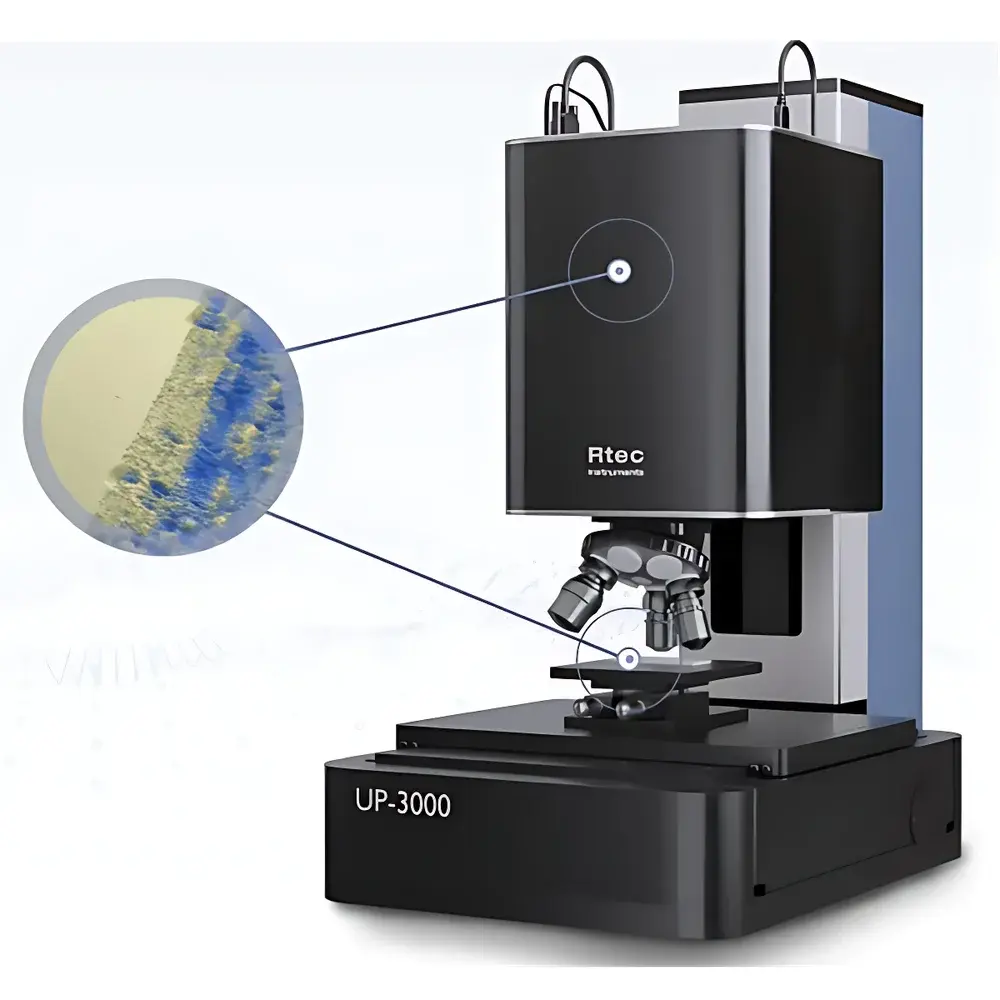
Rtec UP Series Dual-Mode 3D Optical Profilometer
| Brand | Rtec |
|---|---|
| Origin | Switzerland |
| Model | UP Series |
| Measurement Principle | White-Light Interferometry |
| Product Type | Non-Contact Profilometer / Surface Roughness Analyzer |
| Standard Stage | 150 × 150 mm motorized XY stage (optional 210 × 310 mm) |
| Vertical Range | Up to 100 mm |
| Tilt Stage | ±6° |
| XY Stage Resolution | 0.1 µm |
| Imaging Modes | White-Light Interferometry, Rotating-Disk Confocal Microscopy, Dark-Field Microscopy, Bright-Field Microscopy |
| Sensor Heads | Sigma Head (WLI only), Lambda Head (WLI + Confocal + Dark-Field + Bright-Field) |
| Automated Stitching Capability | Yes |
| Software Compliance | ASTM E1250, ISO 25178-2, ISO 4287, USP <1059>, FDA 21 CFR Part 11 audit trail support |
Overview
The Rtec UP Series Dual-Mode 3D Optical Profilometer is an engineered platform for high-fidelity, non-contact surface topography characterization across diverse material classes and geometries. Based on white-light interferometry (WLI) as its primary quantitative metrology engine, the system integrates four complementary optical imaging modalities—WLI, rotating-disk confocal microscopy, dark-field microscopy, and bright-field microscopy—within a single, unified hardware architecture. This multi-modal convergence enables rigorous surface analysis without physical contact or sample preparation, supporting measurements on optically challenging surfaces including transparent substrates (e.g., fused silica, sapphire), highly reflective metals, low-contrast polymer films, curved optics, and nanostructured biomaterials. The instrument operates under controlled environmental conditions and delivers sub-nanometer vertical resolution in WLI mode, with lateral resolution governed by objective magnification and optical diffraction limits. Its modular sensor head design—Sigma (dedicated WLI) and Lambda (full multimodal)—allows users to configure the system according to application-specific metrological requirements while maintaining mechanical and software interoperability.
Key Features
- Single-platform multimodal operation: Seamlessly switch between WLI, confocal, dark-field, and bright-field imaging via software command—no manual reconfiguration or hardware swapping required.
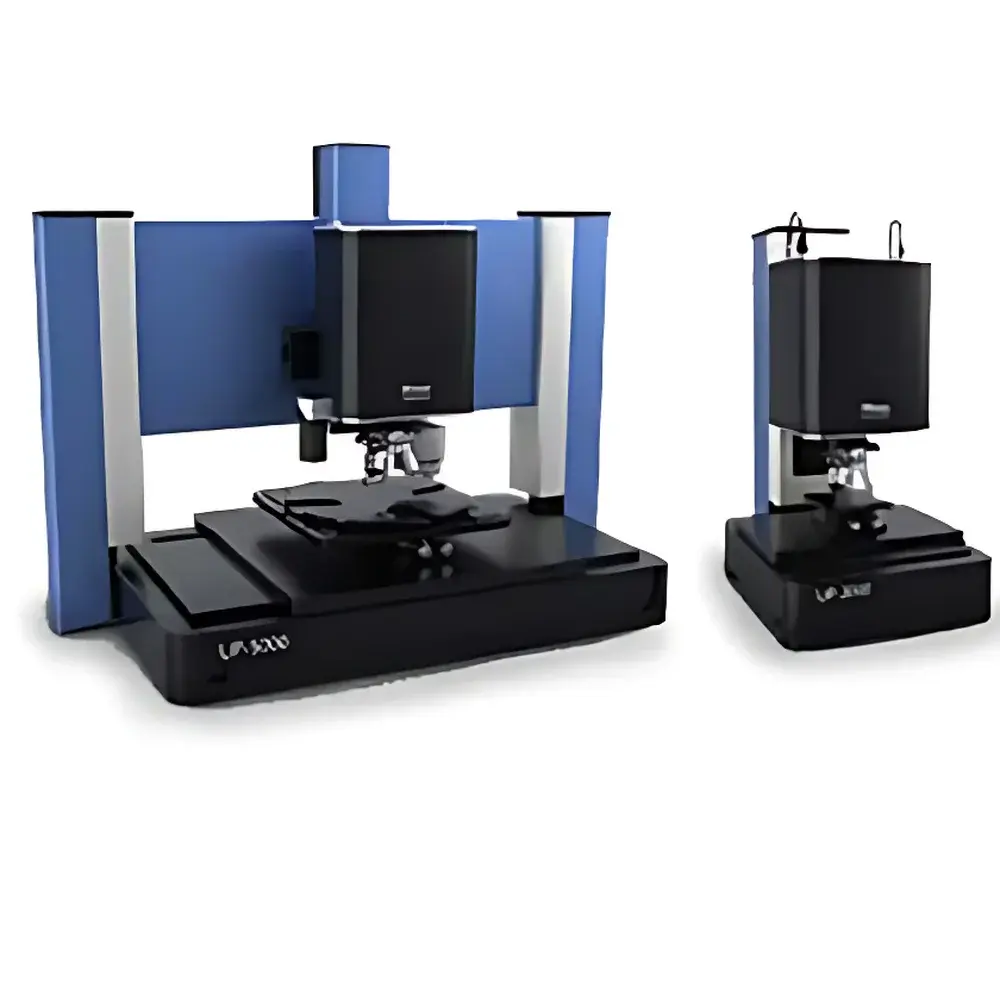
- High-precision motorized stages: Standard 150 × 150 mm XY stage with 0.1 µm encoder resolution; optional extended 210 × 310 mm stage for large-area wafer or substrate mapping.
- Vertical scanning capability up to 100 mm: Enables characterization of deep trenches, MEMS structures, and stepped coatings without Z-axis recalibration.
- Integrated tilt stage (±6°): Facilitates accurate measurement of inclined surfaces and angled microfeatures while preserving optical alignment integrity.
- Automated stitching algorithm: Supports tile-based acquisition across arbitrarily large fields-of-view with sub-pixel registration accuracy and seamless height map merging.
- Dual-head architecture: Sigma head optimized for high-speed, high-repeatability WLI; Lambda head adds confocal sectioning for volumetric profiling and enhanced edge contrast on low-reflectivity surfaces.
Sample Compatibility & Compliance
The UP Series accommodates samples ranging from semiconductor wafers and optical lenses to biomedical implants and tribological test coupons. It supports flat, spherical, cylindrical, and freeform surfaces with radii down to 2 mm. Sample mounting is compatible with standard vacuum chucks, kinematic mounts, and custom fixtures. All measurement workflows adhere to international surface metrology standards—including ISO 25178-2 (areal surface texture parameters), ISO 4287 (profile-based roughness), ASTM E1250 (instrument calibration verification), and USP (surface characterization of pharmaceutical delivery devices). Software includes full 21 CFR Part 11 compliance features: electronic signatures, role-based access control, immutable audit trails, and data integrity validation logs—essential for GLP/GMP-regulated environments.
Software & Data Management
Rtec’s proprietary SurfaceView™ software provides a unified interface for acquisition, real-time visualization, and ISO-compliant analysis. It includes over 200 traceable surface parameters (Sa, Sq, Sz, Vmp, Vmc, etc.), advanced filtering (Gaussian, spline, robust polynomial), grain analysis, layer-thickness extraction (for transparent films), and wear volume quantification via reference-plane subtraction. Data export supports ASCII, CSV, HDF5, and Metrology Exchange Format (MEF) for third-party integration. Batch processing, script automation (Python API), and report generation templates ensure reproducibility across laboratories and regulatory submissions.
Applications
- Thin-film thickness and uniformity mapping on silicon wafers and OLED substrates
- Quantitative wear volume calculation in tribology studies (e.g., DLC-coated ball-on-disk tests)
- Step-height metrology for photolithography process control (e.g., resist development, etch depth)
- Roughness and waviness analysis of machined surfaces per ISO 13565
- Morphological characterization of microfluidic channels, biofilms, and porous scaffolds
- Film delamination and coating failure detection via height discontinuity mapping
- Surface defect classification (scratches, pits, residues) using multi-contrast image fusion
FAQ
What is the minimum resolvable feature size in WLI mode?
The lateral resolution depends on the objective lens used; with a 100× objective, the theoretical diffraction-limited resolution is approximately 0.35 µm. Vertical resolution in WLI is typically ≤0.1 nm RMS under stable environmental conditions.
Can the system measure transparent thin films on silicon substrates?
Yes—WLI leverages interference fringes generated at both air/film and film/substrate interfaces, enabling simultaneous determination of film thickness and substrate topography without destructive cross-sectioning.
Is automated focus finding supported for curved or tilted samples?
Yes—the Lambda head incorporates real-time autofocus algorithms that dynamically adjust Z-position during scan acquisition, even on continuously varying curvature or angular surfaces.
Does the software support custom parameter definitions for internal SOPs?
Yes—SurfaceView™ allows users to define and save custom parameter sets, formulas, and reporting layouts aligned with internal quality protocols or customer-specific deliverables.
How is calibration traceability maintained across instruments?
Each system ships with NIST-traceable step-height and roughness calibration artifacts. Software includes built-in calibration verification routines compliant with ISO/IEC 17025 requirements for accredited metrology labs.