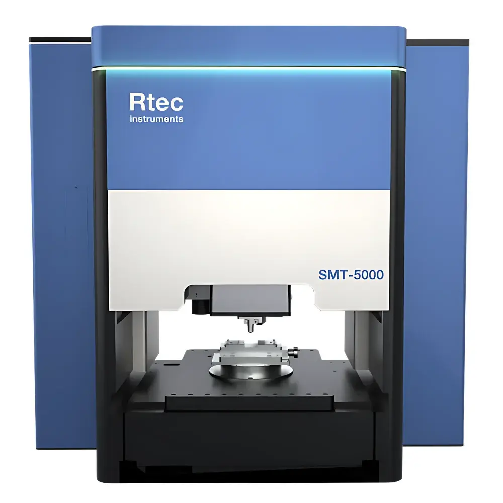
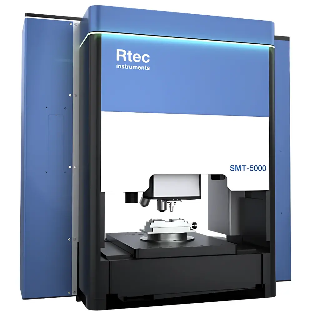
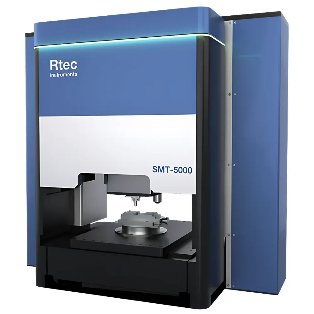
Rtec SMT-5000 Nanoindentation and Scratch Tester
| Brand | Rtec |
|---|---|
| Origin | Switzerland |
| Model | SMT-5000 |
| Instrument Type | Nanoindentation and Scratch Tester |
| Maximum Indentation Depth | 500 µm |
| Effective Load Range | 0.1–200 N |
| Load Resolution | 0.1 N |
| Displacement Range | 100 mm |
| Displacement Resolution | 1 nm |
| Maximum Friction Force | 100 N |
| Indenter Type | Diamond |
Overview
The Rtec SMT-5000 Nanoindentation and Scratch Tester is a high-precision, dual-function mechanical characterization platform engineered for quantitative evaluation of surface and interfacial mechanical properties at micro- and nanoscales. It integrates nanoindentation and controlled scratch testing within a single, rigid, air-bearing-supported frame—enabling simultaneous measurement of hardness, elastic modulus, creep behavior, fracture toughness, adhesion strength, coefficient of friction, and wear resistance. The system operates on the principle of precise force–displacement feedback control using closed-loop piezoelectric actuation and capacitive displacement sensing, ensuring sub-nanometer positional fidelity and real-time load regulation. Designed for research laboratories and industrial quality control environments, the SMT-5000 meets the stringent metrological requirements of advanced thin-film, coating, biomaterial, and semiconductor applications where mechanical integrity under localized stress must be rigorously quantified.
Key Features
- Modular dual-mode operation: seamless switching between nanoindentation (quasi-static and dynamic) and linear/oscillatory scratch testing without hardware reconfiguration.
- Ultra-low thermal drift (<0.1 nm/min) achieved via active temperature stabilization and symmetrical thermal mass design—critical for long-duration creep or relaxation measurements.
- High-force capability with 0.1–200 N load range and 0.1 N resolution, enabling characterization of both soft polymers and hard ceramics, including multilayer stacks and composite interfaces.
- Nanometer-scale displacement resolution (1 nm) over a 100 mm vertical travel range—supporting large-area mapping, cross-sectional profiling, and depth-resolved property gradients.
- Diamond Berkovich, cube-corner, spherical, and Rockwell-type indenters; interchangeable via motorized turret with automated alignment verification.
- Integrated high-speed optical microscopy (5×–100×) and in-situ scanning white-light interferometry for real-time topographic imaging before, during, and after testing.
Sample Compatibility & Compliance
The SMT-5000 accommodates samples up to 300 × 300 × 100 mm (L × W × H) with standard stage clamping, vacuum chuck, or custom fixtures for irregular geometries. It supports conductive and non-conductive substrates—including Si wafers, metallic alloys, polymer films, glass, biomedical implants, and 2D materials—without requiring conductive coating. All test protocols adhere to internationally recognized standards, including ASTM G174 (Standard Test Method for Determining Resistance of Coatings to Scratch by Abrasive Slurry), ASTM G133 (Standard Test Method for Linearly Reciprocating Ball-on-Flat Wear), ISO 14577 (Metallic materials — Instrumented indentation test), and ISO 20519 (Wear testing — Terminology and classification). Data acquisition and reporting modules are compatible with GLP/GMP audit trails and support FDA 21 CFR Part 11-compliant electronic signatures when deployed with validated software configurations.
Software & Data Management
The proprietary MultiTest™ software provides full instrument control, real-time data visualization, and automated analysis workflows. It includes pre-built modules for Oliver–Pharr analysis, pile-up/sink-in correction, Weibull statistics for hardness distribution, critical load determination (Lc) from acoustic emission and friction coefficient inflection, and depth-sensing wear volume calculation. Raw force–displacement curves, video-synchronized scratch traces, and 3D topography maps are stored in vendor-neutral HDF5 format with embedded metadata (test parameters, calibration history, environmental conditions). Export options include CSV, MATLAB .mat, and standardized ASTM E1823-compliant XML schemas. Audit logs record all user actions, parameter changes, and calibration events with timestamps and operator IDs—ensuring traceability for regulatory submissions.
Applications
- Thin-film adhesion assessment in PVD/CVD coatings for aerospace turbine blades and cutting tools.
- Mechanical mapping of graded bioceramic coatings on orthopedic implants to correlate local modulus with osseointegration potential.
- Quantitative wear resistance ranking of automotive clearcoats under simulated grit abrasion per OEM specifications.
- Nanoscale hardness and modulus profiling across semiconductor device cross-sections (e.g., gate stack, BEOL interconnects).
- Time-dependent deformation analysis (creep, stress relaxation) of hydrogels and elastomeric encapsulants used in flexible electronics.
- Interfacial fracture energy estimation in polymer–metal laminates for battery packaging integrity validation.
FAQ
What ASTM standards does the SMT-5000 support for scratch testing?
ASTM G174 (abrasive slurry scratch resistance) and ASTM G133 (ball-on-flat reciprocating wear) are fully implemented through dedicated test templates, including automatic Lc detection algorithms and compliance reporting frameworks.
Can the system perform continuous stiffness measurement (CSM) during indentation?
Yes—the SMT-5000 supports CSM mode with user-defined oscillation amplitude (2–10 nm) and frequency (45–75 Hz), enabling depth-resolved modulus mapping without unloading interruptions.
Is thermal drift compensation performed in real time or post-processing?
Thermal drift is minimized at the hardware level (0 nm/min baseline drift); residual drift is monitored continuously and corrected in real time via active feedback on the displacement signal path.
How is indenter tip geometry verified and calibrated?
Tip geometry is characterized ex situ using SEM-based tip imaging and in situ via area function calibration on fused silica reference samples per ISO 14577 Annex A.
Does the system support third-party automation integration?
Yes—RESTful API and TCP/IP command protocols enable integration with robotic sample handlers, environmental chambers, and MES/LIMS platforms for unattended batch testing.
Related Products


