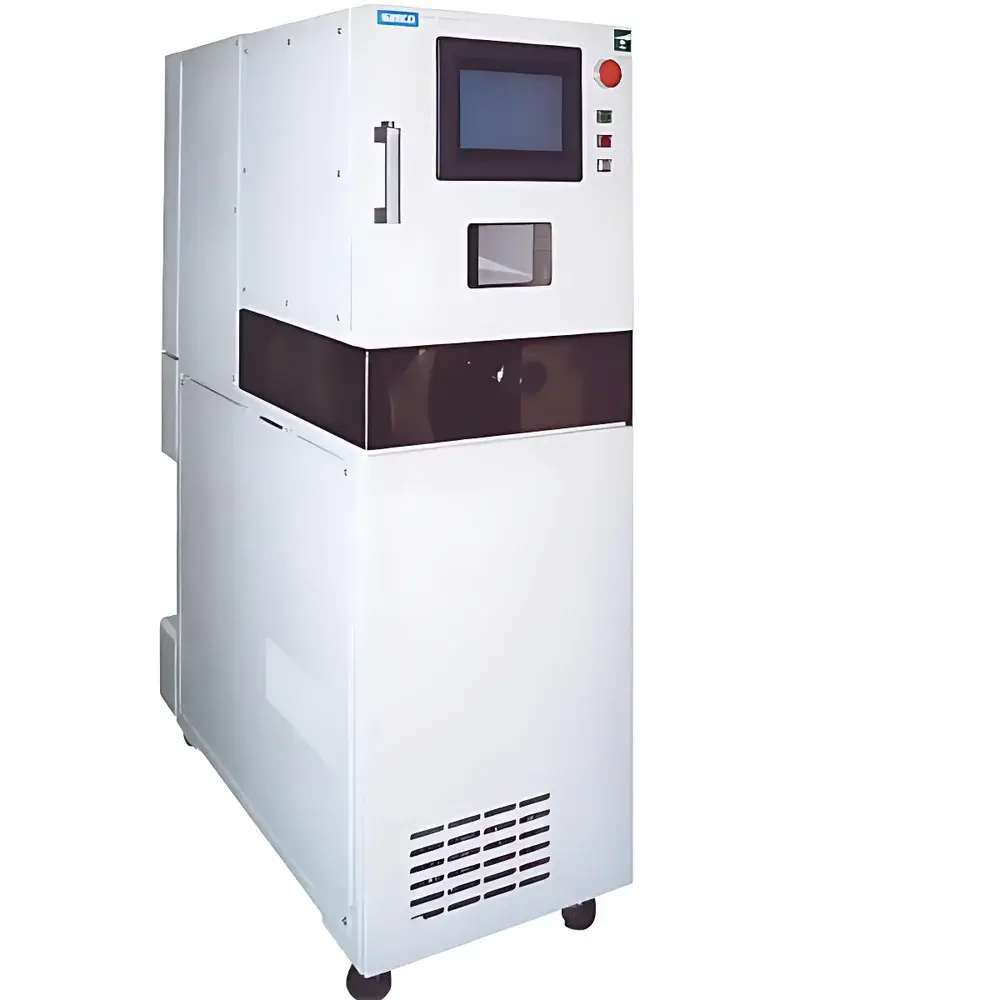
SAMCO PD-220N Plasma-Enhanced Chemical Vapor Deposition (PECVD) System
| Brand | SAMCO |
|---|---|
| Origin | Japan |
| Model | PD-220N |
| Wafer Capacity | 5 × ø3″, 3 × ø4″, or 1 × ø8″ wafers |
| Footprint Reduction | 40% vs. legacy SAMCO PECVD platforms |
| Process Gases | SiH₄, NH₃, N₂O, TEOS (optional add-on), O₂, Ar, N₂ |
| Plasma Source | RF (13.56 MHz) capacitive coupling |
| Chamber Material | Anodized aluminum with quartz-lined process zone |
| Vacuum System | Dry scroll pump + optional turbo-molecular pump |
| Compliance | CE-marked, compatible with ISO 14644-1 Class 5 cleanroom integration |
Overview
The SAMCO PD-220N is a compact, high-reproducibility Plasma-Enhanced Chemical Vapor Deposition (PECVD) system engineered for the controlled synthesis of silicon-based thin films—including silicon dioxide (SiO₂), silicon nitride (Si₃N₄), and hydrogenated amorphous silicon (a-Si:H)—on semiconductor substrates. Unlike thermal CVD, PECVD lowers the required substrate temperature by utilizing radio-frequency (13.56 MHz) plasma to dissociate precursor gases (e.g., SiH₄, NH₃, N₂O, TEOS), enabling high-quality film growth at temperatures as low as 100–300 °C. This capability is critical for temperature-sensitive substrates such as flexible polymers, pre-metallized wafers, or devices incorporating low-k dielectrics or back-end-of-line (BEOL) interconnect stacks. The PD-220N integrates a fully sealed, anodized aluminum reaction chamber with internal quartz lining to ensure plasma uniformity, minimize metallic contamination, and support repeatable stoichiometry control across deposition runs.
Key Features
- Ultra-compact footprint—reduced by 40% compared to prior-generation SAMCO PECVD tools—enabling deployment in space-constrained R&D labs, pilot lines, and shared cleanroom facilities without compromising process integrity.
- Multi-format wafer compatibility: configurable load-lock and chuck design supports simultaneous processing of up to five 76 mm (3″) wafers, three 100 mm (4″) wafers, or one 200 mm (8″) wafer—facilitating rapid process development, DOE validation, and low-volume production transitions.
- Modular gas delivery architecture with mass flow controllers (MFCs) calibrated for SiH₄, NH₃, N₂O, O₂, Ar, and N₂; optional TEOS liquid injection module available for high-purity, low-stress SiO₂ deposition with tunable refractive index (1.44–1.48) and etch rate uniformity <±3% (3σ, across 200 mm).
- RF-powered parallel-plate electrode configuration with impedance-matched matching network ensures stable plasma ignition and sustained power coupling across varying pressure regimes (0.1–10 Torr), supporting both high-rate and low-damage film growth modes.
- Integrated dry vacuum system based on oil-free scroll pumping, with optional turbo-molecular pump upgrade for sub-10⁻⁵ Torr base pressure—essential for minimizing residual hydrocarbon contamination and improving film density and breakdown voltage.
Sample Compatibility & Compliance
The PD-220N accommodates standard semiconductor substrates including bare silicon, SOI, glass, quartz, and sapphire wafers up to 200 mm in diameter. Chuck temperature is actively controlled within ±1 °C over the full operating range (room temperature to 350 °C), ensuring thermal stability during extended depositions. All wetted materials comply with SEMI F57 standards for semiconductor tool construction. The system meets CE safety directives (2014/30/EU EMC, 2014/35/EU LVD) and is designed for seamless integration into ISO 14644-1 Class 5 (ISO Class 5) cleanroom environments. Optional documentation packages support IQ/OQ protocols aligned with ISO 9001 and internal GLP/GMP quality systems.
Software & Data Management
Operation is managed via SAMCO’s proprietary Windows-based control software, featuring recipe-driven automation, real-time plasma parameter logging (forward/reflected RF power, chamber pressure, gas flows, substrate temperature), and event-triggered data capture. All process logs are timestamped and stored in CSV-compatible format with optional SQL database export. Audit trail functionality records user login/logout events, recipe modifications, and manual intervention points—supporting compliance with FDA 21 CFR Part 11 requirements when configured with electronic signature modules and role-based access control.
Applications
- Gate dielectrics and passivation layers in MEMS and power device fabrication
- Anti-reflective coatings (ARC) and interlayer dielectrics (ILD) for photovoltaic cell manufacturing
- Encapsulation barriers for OLED and flexible display backplanes
- Low-temperature SiNₓ stress tuning for CMOS image sensor microlens stacks
- Rapid prototyping of multilayer stacks (e.g., SiO₂/SiNₓ/SiO₂) in academic and industrial thin-film research
FAQ
What maximum film thickness uniformity can be achieved on 200 mm wafers?
Typical thickness non-uniformity is ≤±3.5% (1σ, measured by ellipsometry at 49 points), verified using blanket SiO₂ deposition at 200 °C, 2.5 Torr, and 150 W RF power.
Is remote monitoring or integration with factory MES systems supported?
Yes—the system provides Ethernet-based SECS/GEM interface (SEMI E30/E37 compliant) for host communication, enabling automated job dispatch, status reporting, and alarm forwarding to central manufacturing execution systems.
Can the PD-220N deposit carbon-based films such as a-C or SiC?
While optimized for silicon-containing precursors, the platform supports CH₄, C₂H₂, and TMS (tetramethylsilane) with appropriate MFC calibration and chamber conditioning; process qualification required per material system.
What maintenance intervals are recommended for the RF generator and vacuum components?
RF matching network inspection every 500 hours; dry pump oil replacement every 3,000 hours (scroll pump); quartz liner cleaning after every 50 SiO₂ runs or upon visible coating buildup.
Related Products


