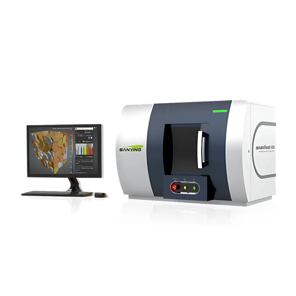
Sanying Precision nanoVoxel-1000 Desktop Micro-CT System
| Brand | Sanying Precision |
|---|---|
| Origin | Tianjin, China |
| Model | nanoVoxel-1000 |
| Detector Type | Flat-Panel Detector |
| Scan Mode | Translation-Rotation (TR) |
| Spatial Resolution | 2 µm |
| Detail Resolution Capability | 300 nm |
| X-ray Source | Sealed-Tube |
| Maximum Tube Voltage | 110 kV |
| Field of View (FoV) | 300 mm (diameter) × 200 mm (height) |
| Sample Weight Capacity | 15 kg |
| System Dimensions (L×W×H) | 900 mm × 500 mm × 660 mm |
| Detector Active Area | 145 mm × 114 mm |
| Detector Pixel Matrix | 2940 × 2304 |
| System Mass | 500 kg |
Overview
The Sanying Precision nanoVoxel-1000 is a high-performance desktop micro-computed tomography (micro-CT) system engineered for non-destructive 3D internal structure characterization at sub-micron detail resolution. Leveraging cone-beam geometry and high-stability sealed-tube X-ray source technology, the system operates on the principle of X-ray attenuation-based volumetric reconstruction—acquiring hundreds to thousands of projection images across a full 360° rotation (combined with precise linear translation in TR mode), followed by filtered back-projection or iterative reconstruction algorithms to generate isotropic 3D voxel datasets. Designed for laboratory environments with space constraints—including university core facilities, materials R&D labs, and industrial QA/QC departments—the nanoVoxel-1000 delivers metrologically traceable dimensional analysis, porosity quantification, defect detection, and phase segmentation without sample sectioning or coating. Its compact footprint (under 0.5 m² floor area) and robust mechanical architecture—including passive vibration isolation—enable stable operation in non-dedicated rooms and mobile deployment scenarios such as marine research vessels or field-deployable inspection units.
Key Features
- Sub-micron detail resolution capability down to 300 nm, validated using certified line-pair test objects per ISO 15739 and ASTM E2737 standards
- Sealed-tube X-ray source (max. 110 kV, air-cooled) eliminating filament replacement and gas refills—reducing total cost of ownership and downtime
- High-dynamic-range flat-panel detector (145 mm × 114 mm active area, 2940 × 2304 pixels) enabling high-fidelity low-contrast imaging of polymer composites, foams, ceramics, and light-metal alloys
- Translation-rotation (TR) scanning geometry optimized for geometric magnification control and reduced cone-beam artifacts in medium-field-of-view acquisitions
- Integrated mechanical stability package: granite baseplate, precision air-bearing rotation stage, and multi-layer passive damping—supporting reproducible measurements under ambient lab conditions (±1 °C, <50% RH)
- Modular shielding design compliant with IEC 61331-1 for operator safety; optional lead-acrylic viewing window available for real-time alignment verification
Sample Compatibility & Compliance
The nanoVoxel-1000 accommodates samples up to 300 mm in diameter and 200 mm in height, with maximum mass of 15 kg—suitable for battery cells, turbine blade cooling channels, additive-manufactured lattice structures, geological core plugs, and electronic encapsulation assemblies. It supports both absorption-contrast and phase-contrast enhanced imaging modes (via edge-enhancement post-processing) for low-Z materials including polymers, biological tissues, and carbon-fiber composites. System software enforces ALARA (As Low As Reasonably Achievable) exposure protocols and logs all acquisition parameters—including kV, µA, exposure time, number of projections, and geometric magnification—for audit-ready documentation. The platform conforms to ISO/IEC 17025 requirements for calibration traceability and supports GLP-compliant workflow execution when paired with optional electronic lab notebook (ELN) integration modules.
Software & Data Management
Acquisition, reconstruction, and analysis are unified within the proprietary nanoVoxel Control Suite v4.x—a Windows-based application supporting DICOM 3.0 export, NIfTI compatibility, and HDF5 binary output for large-volume dataset handling. Reconstruction leverages GPU-accelerated Feldkamp-Davis-Kress (FDK) and SART algorithms with ring artifact suppression, beam hardening correction, and automatic center-of-rotation calibration. Post-processing tools include threshold-based segmentation, pore network modeling (using maximal ball algorithm), wall thickness mapping (local thickness transform), and quantitative morphometry (BET surface area, tortuosity, connectivity density). All processing steps generate immutable metadata logs compliant with FDA 21 CFR Part 11 requirements—including user ID, timestamp, parameter set hash, and audit trail export functionality.
Applications
- Materials science: Quantitative analysis of sintering homogeneity in metal powders, interfacial debonding in thermal barrier coatings, and crack propagation kinetics in ceramic matrix composites
- Electronics: Void detection in solder joints, wire bond integrity assessment, and conformal coating uniformity evaluation
- Energy: Electrode tortuosity measurement in Li-ion battery anodes, separator pore distribution mapping, and catalyst layer thickness profiling
- Geosciences: Digital rock physics modeling via fluid flow simulation on segmented pore spaces derived from reservoir core samples
- Additive manufacturing: As-built dimensional deviation reporting against CAD models, powder removal validation, and support structure residual stress estimation
FAQ
What is the difference between spatial resolution and detail resolution in micro-CT?
Spatial resolution refers to the smallest resolvable distance between two points in reconstructed voxel space (typically measured using modulation transfer function or line-pair test charts), while detail resolution indicates the finest observable feature in raw projection data—often limited by focal spot size, detector pixel pitch, and geometric magnification. The nanoVoxel-1000 achieves 2 µm spatial resolution and 300 nm detail resolution under optimal magnification and exposure conditions.
Can the system perform in-situ mechanical testing during scanning?
Yes—the nanoVoxel-1000 features standardized 80-mm-diameter top and bottom access ports compatible with third-party miniaturized load frames (e.g., Deben tensile stages), enabling dynamic 4D CT experiments up to 5 kN axial load with synchronized motion control and projection triggering.
Is the system qualified for ISO 17025-accredited laboratories?
The nanoVoxel-1000 includes factory calibration certificates traceable to NIST standards for geometric magnification, spatial linearity, and X-ray beam stability. Optional annual performance verification packages—performed by Sanying-certified engineers—provide documented evidence meeting ISO/IEC 17025 clause 6.4.10 requirements for equipment monitoring.
Does the software support automated batch processing of multiple samples?
Yes—via Python API integration (PyVoxel), users can script fully unattended workflows covering stage positioning, scan parameter loading, reconstruction queue submission, and post-processing pipeline execution—including conditional logic based on real-time image quality metrics.


