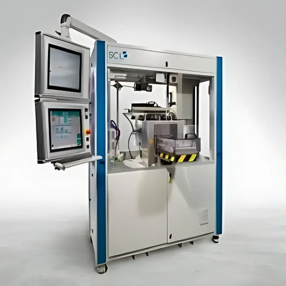
SCIL LabSCIL Nanoimprint Lithography System
| Brand | SCIL |
|---|---|
| Origin | Netherlands |
| Model | LabSCIL |
| Wafer Size | Up to 8-inch (200 mm) |
| Alignment Accuracy | < 1 µm |
| Imprint Technology | Low-Force Soft-Mold Substrate-Conformal Nanoimprint |
| Compatible Resists | Thermal Sol-Gel, UV Sol-Gel, UV Organic |
| Wafer Thickness Range | 0.3–2.5 mm |
| Footprint (W×L×H) | 1.8 × 1.4 × 2.2 m |
| Resist Application | External Spin-Coater Required |
| Compliance | Designed for ISO Class 5–7 cleanroom integration |
| Software | SCIL Control Suite with Audit Trail & Parameter Logging |
Overview
The SCIL LabSCIL Nanoimprint Lithography System is a research-grade, benchtop-capable nanoimprint platform engineered for precision patterning at sub-10 nm feature resolution on non-planar and curved substrates. Developed by SCIL (Substrate-Conformal Imprint Lithography), a Netherlands-based spin-off from Philips with deep roots in advanced lithography R&D, the LabSCIL implements the proprietary SCIL process—a hybrid imprint methodology that merges the fidelity of small-area hard mold contact with the scalability and conformality of large-area soft elastomeric stamping. Unlike conventional thermal or UV-NIL systems constrained by substrate flatness or residual layer uniformity, LabSCIL achieves true substrate-conformal contact through controlled low-force compression and adaptive mold deformation, enabling high-fidelity replication across topographically complex surfaces without mechanical damage to wafers or stamps. The system is purpose-built for process development, materials evaluation, and low-volume prototyping in academic labs, national research institutes, and semiconductor equipment suppliers—serving as a bridge between fundamental nanofabrication research and pilot-line qualification.
Key Features
- Substrate-conformal imprint capability: Maintains full pattern fidelity on substrates with curvature, warpage, or surface topography up to ±5 µm deviation over 8-inch wafers.
- Proven <10 nm half-pitch resolution: Validated using certified NIST traceable line/space gratings and verified via SEM/AFM metrology.
- Alignment accuracy <1 µm (3σ): Achieved via integrated high-magnification optical alignment subsystem with motorized stage compensation and real-time fiducial tracking.
- Multi-resist compatibility: Supports thermal sol-gel (crosslinking at 120–180 °C), UV-curable sol-gel (365 nm LED source), and standard UV organic resists—enabling direct functionalization without etch transfer in select applications.
- Low-force imprint architecture: Peak contact pressure <100 kPa, minimizing template wear and eliminating substrate fracture risk on thin or fragile substrates (e.g., SOI, GaN-on-sapphire).
- Cleanroom-ready mechanical design: Stainless steel frame, vibration-isolated granite base, and HEPA-filtered internal purge path compliant with ISO 5–7 environments.
Sample Compatibility & Compliance
The LabSCIL accommodates silicon, SiC, GaN, quartz, fused silica, and flexible polymer substrates (e.g., PI, PET) ranging from 2-inch to 8-inch diameter and 0.3–2.5 mm thickness. Its conformal contact mechanism eliminates the need for global planarization, making it suitable for heterogeneous integration stacks and MEMS packaging substrates. All hardware and software modules are designed to support GLP and GMP-aligned workflows: resist dispensing parameters, temperature ramps, UV dose, pressure profiles, and alignment offsets are timestamped and logged with user ID attribution. The system architecture supports optional 21 CFR Part 11-compliant electronic signatures and audit trail export when integrated with validated laboratory information management systems (LIMS). Process recipes may be qualified per ASTM E2921 (Standard Guide for Nanoscale Pattern Characterization) and ISO/IEC 17025 calibration traceability protocols.
Software & Data Management
The SCIL Control Suite provides deterministic, scriptable operation via a Windows-based GUI with dual-mode interface: guided wizard mode for rapid setup and expert mode for granular parameter control (e.g., ramp rate, dwell time, vacuum sequencing, UV intensity modulation). All imprint cycles generate structured XML metadata including environmental logs (chamber temp/humidity), force vs. displacement curves, real-time alignment residuals, and resist cure status. Raw data exports comply with HDF5 and CSV standards for post-processing in MATLAB, Python (SciPy), or industry metrology suites (e.g., KLA-CMS, Bruker NanoScope Analysis). Remote monitoring and diagnostics are supported via secure TLS-encrypted Ethernet connection; no cloud dependency or vendor-hosted infrastructure is required.
Applications
- Development of high-aspect-ratio plasmonic metasurfaces for IR sensing and beam shaping.
- Direct patterning of sol-gel dielectrics as antireflective, waveguide, or passivation layers—bypassing deposition and dry etch steps.
- Prototyping of photonic crystal cavities and ring resonators on non-planar III-V platforms.
- Roll-to-plate and wafer-level imprint process transfer studies for hybrid integration of micro-optics with CMOS image sensors.
- Fabrication of bio-compatible nanostructured surfaces for cell adhesion control and lab-on-chip fluidic channel definition.
- Maskless fabrication of diffractive optical elements (DOEs) on curved ophthalmic lenses and automotive HUD substrates.
FAQ
Does LabSCIL support automated resist dispensing?
No—resist application is performed externally using a standard spin coater; LabSCIL focuses exclusively on imprint, alignment, and cure functions.
Can LabSCIL be upgraded to handle 12-inch wafers?
No—LabSCIL is mechanically and optically optimized for ≤8-inch substrates; SCIL’s production-grade systems (e.g., FabSCIL) support 300 mm wafers.
Is thermal sol-gel resist supplied with the system?
SCIL provides material specifications and processing guidelines; resist procurement is handled directly through SCIL-approved chemical partners under NDA.
What level of cleanroom classification is required?
ISO Class 5 is recommended for optimal particle control during manual loading; ISO Class 7 is acceptable if combined with localized laminar flow hoods.
How is template lifetime quantified for thermal sol-gel processes?
Under typical LabSCIL operating conditions (≤100 kPa, 150 °C, N₂ ambient), SCIL reports >500 imprint cycles with <3% linewidth variation measured by CD-SEM.


