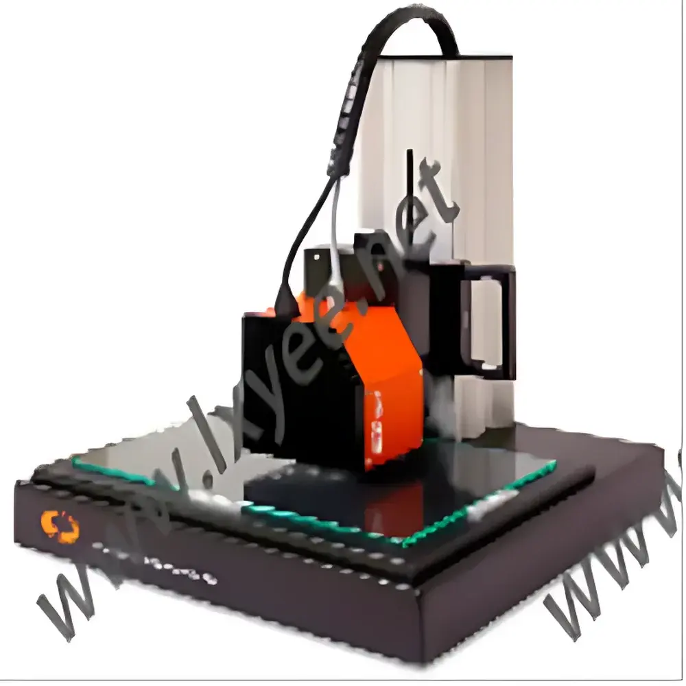


SENTECH MDPspot Desktop Minority Carrier Lifetime Tester
| Brand | SENTECH |
|---|---|
| Origin | Germany |
| Model | MDPspot |
| Type | Contactless, Microwave Photoconductance Decay (μ-PCD) Based Lifetime Tester |
| Sample Handling | Manual Z-axis adjustment (up to 156 mm height) |
| Measurement Mode | Single-point, non-contact, room-temperature operation |
| Material Compatibility | Crystalline and multicrystalline silicon wafers & bricks |
| Compliance | Designed for R&D and process monitoring in PV and semiconductor fabrication environments |
| Software | MDP Control Suite (Windows-based, real-time visualization, CSV export, GLP-compliant data logging) |
Overview
The SENTECH MDPspot is a compact, desktop-class minority carrier lifetime tester engineered for rapid, non-destructive characterization of crystalline and multicrystalline silicon materials used in photovoltaic (PV) cell manufacturing and semiconductor R&D. It employs microwave photoconductance decay (μ-PCD), a well-established, contactless technique standardized in ASTM F1534 and IEC 62788-5-1, to quantify effective minority carrier lifetime (τeff) with high reproducibility. Unlike laser beam induced current (LBIC) or quasi-steady-state photoconductance (QSSPC) systems, μ-PCD enables single-point lifetime assessment without surface passivation or electrical contacts—making it ideal for inline process control across ingot growth, wafering, texturing, diffusion, and metallization stages. The system operates at ambient temperature and requires no vacuum or cryogenic infrastructure, significantly reducing operational overhead while maintaining measurement fidelity suitable for statistical process control (SPC) and yield correlation studies.
Key Features
- Contactless μ-PCD measurement principle ensures no sample damage, no surface preparation, and minimal operator dependency.
- Manually adjustable Z-axis stage accommodates samples up to 156 mm in height—including full-size silicon bricks, pseudo-square wafers, and thin substrates—without mechanical recalibration.
- Integrated optional four-point probe module enables simultaneous resistivity (ρ) measurement on the same location, supporting dopant uniformity evaluation per ASTM F84.
- Compact footprint (≤0.5 m²) and low power consumption (<150 W) allow deployment in cleanroom-adjacent labs, pilot lines, or quality control stations.
- Real-time signal acquisition with ≥100 kHz sampling rate ensures robust decay curve fitting using multi-exponential analysis algorithms.
- Calibration traceable to NIST-traceable reference wafers; system stability verified via daily drift monitoring protocols.
Sample Compatibility & Compliance
The MDPspot supports bare, textured, or coated silicon specimens—regardless of crystal orientation (Czochralski, float-zone, or cast multicrystalline). It is validated for use with standard 156 × 156 mm², 166 × 166 mm², and 182 × 182 mm² wafers, as well as rectangular bricks up to 220 mm wide. No front-side metallization or anti-reflection coating removal is required. The instrument complies with electromagnetic compatibility (EMC) directive 2014/30/EU and low-voltage directive 2014/35/EU. Its measurement methodology aligns with ISO 12099:2017 (photovoltaic devices — procedures for measuring minority-carrier lifetime) and supports audit-ready documentation for ISO 9001, IATF 16949, and PVQAP-certified production facilities.
Software & Data Management
The MDP Control Suite provides intuitive Windows-based operation with dual-view interface: live waveform display and τeff map generation (for scanned datasets). All measurements include timestamp, operator ID, sample ID, ambient temperature/humidity metadata, and raw decay traces stored in HDF5 format. Export options include CSV, PNG, and PDF reports compliant with GLP requirements. Audit trail functionality logs all parameter changes, user logins, and calibration events—fully compatible with FDA 21 CFR Part 11 when deployed with validated Windows OS configurations and electronic signature modules.
Applications
- Ingot-to-wafer quality screening: early detection of bulk defects, oxygen precipitates, and metal contamination gradients.
- Process development: quantifying lifetime improvement after gettering, hydrogenation, or surface passivation treatments.
- Material qualification: batch acceptance testing for feedstock silicon, recycled wafers, and epitaxial layers.
- R&D correlation studies: linking τeff values with implied VOC (iVOC), diffusion length, and final cell efficiency.
- Failure analysis: isolating lifetime-limiting mechanisms in degraded modules or field-failed cells via cross-sectional brick mapping.
FAQ
Is the MDPspot suitable for measuring lifetime on textured or saw-damaged surfaces?
Yes. The microwave coupling is insensitive to surface topography, enabling reliable measurements on as-cut, diamond-wire-sawn, or alkaline-textured wafers without planarization.
Can the system be upgraded to support automated XY scanning?
No—the MDPspot is purpose-built as a manual single-point platform. For automated mapping, SENTECH offers the MDPmap series, which shares identical μ-PCD core electronics and software architecture.
Does the resistivity option require physical contact with the sample?
Yes—the integrated four-point probe module makes direct ohmic contact; however, probe placement is fully decoupled from the μ-PCD measurement spot, allowing independent or co-located evaluation.
What calibration standards are recommended for routine verification?
SENTECH supplies certified reference wafers with NIST-traceable lifetime values (e.g., 1–1000 µs range) and resistivity standards per ASTM F84 Annex A1.
Is remote diagnostics or firmware update supported?
Yes—via secure HTTPS-based connection to SENTECH’s engineering portal; updates preserve all user-defined configurations and historical database integrity.


