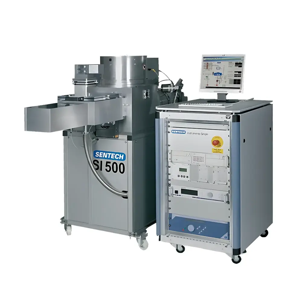
SENTECH SI 500 ICP-RIE Etching System
| Origin | Germany |
|---|---|
| Manufacturer Type | Authorized Distributor |
| Origin Category | Imported |
| Model | SI 500 |
| Price | USD 295,000 (FOB Hamburg) |
| RF Source Frequency | 13.56 MHz |
| ICP Power | 1200 W |
| Bias RF Power | 600 W |
| Plasma Source | Planar Triple Spiral Antenna (PTSA) |
| Endpoint Detection | Interferometric In-situ Monitoring |
| Vacuum System | High-throughput Dry Pumping with Independent Gas Flow & Pressure Control |
| Software | SENTECH Advanced Plasma Process Control (APPC) v5.x |
Overview
The SENTECH SI 500 is a high-performance inductively coupled plasma reactive ion etching (ICP-RIE) system engineered for precision nanofabrication in compound semiconductor and micro-optical device manufacturing. It employs dual-frequency plasma generation—13.56 MHz ICP excitation for high-density plasma production and independent 13.56 MHz bias RF for controlled ion energy delivery—to achieve exceptional etch rate uniformity, anisotropy, and material selectivity. The core innovation lies in its Planar Triple Spiral Antenna (PTSA), a patented planar ICP source that delivers radially symmetric plasma density distribution (>95% uniformity across 200 mm wafers), minimizing edge effects and enabling reproducible high-aspect-ratio patterning. Unlike conventional helical or coil-based ICP sources, the PTSA’s low-inductance, multi-turn geometry reduces parasitic capacitive coupling, suppresses arcing, and enhances plasma stability under aggressive chemistries (e.g., Cl₂/BCl₃ for GaAs, SF₆/CHF₃ for SiO₂). Designed for integration into cleanroom environments, the SI 500 supports wall-mount (penetrating-wall) installation to conserve floor space and reduce vibration coupling—critical for sub-100 nm feature definition.
Key Features
- Planar Triple Spiral Antenna (PTSA): Engineered for uniform plasma density distribution and scalable power coupling up to 1200 W at 13.56 MHz.
- Dual-frequency RF architecture: Independent control of ICP source power (1200 W) and substrate bias power (600 W) enables decoupled optimization of ion flux and ion energy.
- In-situ interferometric endpoint detection: Real-time optical monitoring of etch depth and layer removal via broadband interferometry (400–800 nm), supporting closed-loop process termination with ±2 nm resolution.
- Integrated automatic impedance matching network: Ensures >95% RF power transfer efficiency across varying process conditions and chamber states.
- Circulating gas injection manifold: Gas delivery integrated directly into the PTSA structure ensures laminar, radial flow distribution and eliminates shadowing effects from discrete showerheads.
- High-throughput dry vacuum system: Dual-stage pumping architecture with independent pressure regulation (1–100 mTorr range) and fast pump-down (<60 s to 10⁻⁶ mbar base pressure).
Sample Compatibility & Compliance
The SI 500 accommodates wafers up to 200 mm diameter (standard configuration) with optional upgrade to 300 mm. It supports diverse substrate materials including GaAs, InP, GaN, SiC, SiO₂, SiNₓ, and polymer resists (e.g., PMMA, HSQ). Chamber materials—alumina-coated aluminum and quartz viewports—ensure chemical inertness during halogen- and fluorine-based chemistries. The system complies with CE Machinery Directive 2006/42/EC, EMC Directive 2014/30/EU, and IEC 61000-6-2/6-4 immunity/emission standards. Process recipes are fully traceable and support audit-ready documentation per ISO 9001:2015 and ISO/IEC 17025 requirements. Optional FDA 21 CFR Part 11-compliant software modules provide electronic signature, audit trail, and role-based access control for regulated R&D and pilot-line environments.
Software & Data Management
SENTECH Advanced Plasma Process Control (APPC) v5.x provides full system orchestration via Windows-based GUI with real-time parameter visualization, recipe management, and automated sequence execution. All process data—including RF forward/reflected power, chamber pressure, gas flow rates, endpoint signal traces, and temperature logs—are timestamped and stored in SQLite-based local databases with configurable export to CSV or HDF5 formats. APPC supports OPC UA connectivity for integration into factory-level MES/SCADA systems. Version-controlled recipe libraries enable cross-platform consistency between development, qualification, and production tools. Remote diagnostics and firmware updates are supported over secure TLS-encrypted connections, with configurable firewall policies for IT compliance.
Applications
- High-aspect-ratio etching of III-V photonic crystals and distributed Bragg reflectors (DBRs) for VCSELs and tunable lasers.
- Anisotropic patterning of GaN HEMT gate recesses and ohmic contact vias with sub-5 nm sidewall roughness.
- Low-damage etching of InP-based modulators and integrated Mach-Zehnder interferometers (MZIs).
- Deep silicon etching for MEMS resonators and micro-opto-electro-mechanical systems (MOEMS).
- Sub-100 nm critical dimension (CD) transfer from e-beam resist into SiO₂ hard masks for EUV lithography development.
FAQ
What wafer sizes does the SI 500 support?
Standard configuration supports 100 mm, 150 mm, and 200 mm wafers; 300 mm capability is available as a factory-installed option with upgraded chuck and chamber liner.
Is the PTSA source compatible with oxygen-based chemistries for polymer resist stripping?
Yes—the PTSA’s low-voltage operation and uniform plasma profile enable stable O₂/Ar plasma generation without electrode erosion or chamber contamination, achieving >1.5 µm/min ash rates with <2% CD loss on patterned photoresist.
How is endpoint detection calibrated for multilayer stacks?
APPC v5.x includes a built-in calibration wizard that acquires reference interferograms from blanket films and auto-generates spectral templates; users may define up to eight simultaneous layer interfaces per recipe.
Does the system support remote operation in unattended mode?
Yes—fully automated batch processing, email/SMS alerting on process completion or fault events, and encrypted VNC access are enabled by default.
What maintenance intervals are recommended for the PTSA source and RF components?
Plasma-facing PTSA components require inspection every 500 hours; RF matching network capacitors are rated for >10,000 hours under continuous operation; full preventive maintenance is scheduled annually per SENTECH Service Manual SM-SI500-Rev4.2.


