Shashin Kagaku PV Cell Busbar & Finger Profile Metrology System
| Brand | Shashin Kagaku |
|---|---|
| Origin | Japan |
| Model | PV Cell Grid Line 3D Profilometer |
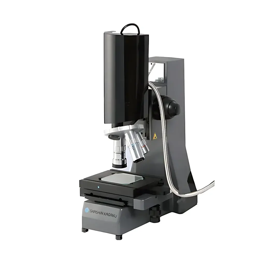
| Measurement Principle | White-Light Interferometry |
| Light Source Options | White LED (430–700 nm, >50,000 h), Tungsten-Halogen (400–900 nm, 10,000 h), Deuterium-Halogen (220–900 nm, 1,000 h) |
| Objective Lenses | 1× (FOV 6.6 × 8.8 mm, Optical Resolution 11 µm, Working Distance 15 mm), 5× (FOV 1.32 × 1.76 mm, Optical Resolution 2.3 µm, Working Distance 4 mm), 50× (FOV 0.132 × 0.176 mm, Optical Resolution 0.51 µm, Working Distance 3 mm) |
| Measurement Capabilities | Simultaneous 3D topography, line width (LW), line height (LH), sidewall angle, step height, roughness (Sa, Sq), and edge definition for metallized grid lines on silicon solar cells |
Overview
The Shashin Kagaku PV Cell Busbar & Finger Profile Metrology System is a non-contact, high-resolution white-light interferometric profilometer engineered for precise 3D dimensional characterization of photovoltaic metallization structures. Designed specifically for R&D laboratories and inline process control environments in solar cell manufacturing, the system quantifies critical geometric parameters—including busbar and finger line width, height, aspect ratio, sidewall profile, and surface topography—without physical contact or sample preparation. Its optical architecture leverages coherence-controlled interference fringe analysis to resolve sub-micron vertical features and lateral dimensions down to 0.51 µm (with 50× objective), enabling traceable, repeatable metrology compliant with industry-recognized dimensional stability requirements for screen-printed, plated, and inkjet-deposited grid lines on mono- and multi-crystalline Si wafers.
Key Features
- Multi-wavelength illumination options optimized for silicon surface reflectivity and anti-reflection coating compatibility: long-life white LED (430–700 nm), broadband tungsten-halogen (400–900 nm), and deep-UV-capable deuterium-halogen (220–900 nm).
- Modular objective turret supporting three calibrated magnifications (1×, 5×, 50×) with documented field-of-view, optical resolution, and working distance specifications for method transfer across labs and production shifts.
- Real-time interferogram acquisition and phase-shifting algorithm for nanometer-level vertical resolution (≤0.1 nm RMS noise floor typical) and sub-pixel lateral registration accuracy.
- Vibration-isolated optical baseplate and passive thermal stabilization to maintain measurement repeatability (<0.3% RSD over 8-hour operation) under ambient lab conditions.
- Integrated motorized XYZ stage with programmable scan patterns (raster, line, point-grid) and auto-focus functionality for unattended batch profiling of full-cell or half-cell substrates up to 210 × 210 mm.
Sample Compatibility & Compliance
The system accommodates standard photovoltaic substrates including textured monocrystalline and multicrystalline silicon wafers (156–210 mm formats), glass/ITO heterojunction (HJT) samples, and perovskite-on-silicon tandem device stacks. Surface finish ranges from as-cut wafer roughness (Ra ≈ 0.5–1.2 µm) to polished passivation layers (SiNx, AlOx) and metal films (Ag, Cu, Ni/Cu). All measurement protocols adhere to ASTM E2921–22 (“Standard Practice for Measuring Critical Dimensions of Photovoltaic Metallization”) and support traceability to NIST-traceable step-height standards. Data integrity meets GLP/GMP documentation requirements, with audit-ready metadata logging (operator ID, timestamp, instrument configuration, environmental conditions).
Software & Data Management
Control and analysis are performed via Shashin Kagaku’s proprietary MetroView™ software suite (v5.2+), which provides ISO/IEC 17025-aligned reporting templates, customizable pass/fail criteria per IEC 61215-2 MQT 17, and automated generation of cross-sectional profiles, 3D surface maps, and statistical process control (SPC) charts. Raw interferometric data is stored in HDF5 format with embedded calibration metadata; export options include CSV, STEP AP214, and GD&T-compliant PDF reports. The software supports FDA 21 CFR Part 11 compliance through role-based access control, electronic signatures, and immutable audit trails for all measurement sessions and parameter modifications.
Applications
- Quantification of screen-printing paste rheology impact on finger line collapse and height uniformity across wafer batches.
- Process window validation for electroplating parameters (current density, bath composition) via real-time line height and aspect ratio monitoring.
- Root-cause analysis of soldering-induced microcracks by correlating local grid line deformation with thermal stress simulation outputs.
- Qualification of new metallization inks (e.g., low-Ag, Ag-free formulations) through comparative 3D morphology analysis against baseline reference cells.
- Supporting ISO 9001-certified quality systems with SPC-ready data for Cp/Cpk calculation on critical-to-quality (CTQ) dimensions such as busbar height tolerance (±1.5 µm).
FAQ
What is the minimum measurable line height for fine-pitch fingers using the 50× objective?
The system achieves reliable detection of step heights ≥0.2 µm with ≤1.5 nm vertical repeatability under controlled environmental conditions.
Can the system measure through anti-reflective coatings (e.g., SiNx) without signal degradation?
Yes—the deuterium-halogen source enables robust interference contrast on coated surfaces due to its broad spectral coverage extending into the UV, where SiNx exhibits higher dispersion and lower absorption.
Is calibration traceable to national metrology institutes?
All vertical scale calibrations are performed using NIST-traceable step-height standards (0.1 µm, 1 µm, 5 µm steps); lateral calibration uses certified grating standards with ±0.02 µm uncertainty.
Does the software support automated defect flagging based on profile deviations?
Yes—MetroView™ includes configurable rule-based anomaly detection that triggers alerts when line width variation exceeds user-defined thresholds or when sidewall angle deviates beyond ±2° from nominal.
What environmental conditions are required for optimal performance?
Recommended operating range: 20–25 °C ambient temperature, <50% RH, and vibration isolation per ISO 20486 Class 2; no active cooling or cleanroom enclosure required.


