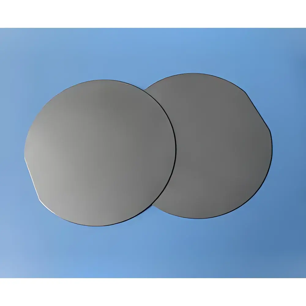
Silicon-Germanium (Si-Ge) Single-Crystal Substrate Wafers
| Brand | Hefei Kejing |
|---|---|
| Origin | Anhui, China |
| Manufacturer Type | Authorized Distributor |
| Origin Category | Domestic |
| Model | Si-Ge (2 wt% Ge) |
| Conductivity Type | P-type |
| Resistivity | 7–8 Ω·cm |
| Surface Finish | Single-side polished |
| Standard Orientation | <100> |
| Standard Dimensions | Ø100 mm × 0.5 mm |
| Packaging | Class 1000 Cleanroom / Class 100 Clean Bag |
| Customization | Available for orientation, diameter, thickness, and double-side polish upon request |
Overview
Silicon-Germanium (Si-Ge) single-crystal substrate wafers are engineered for high-precision epitaxial growth, thin-film deposition, and advanced semiconductor device fabrication. As a lattice-matched or strain-engineered platform for heterostructure integration, Si-Ge substrates enable controlled bandgap tuning, enhanced carrier mobility, and improved thermal mismatch management—particularly critical in Si-based heterojunction bipolar transistors (HBTs), strained-silicon CMOS, and integrated photonics platforms. Unlike sapphire (Al2O3) substrates—which serve distinct roles in wide-bandgap III–V nitride LED/LD epitaxy—the Si-Ge wafer leverages the mature silicon infrastructure while introducing graded compositional flexibility (here specified at 2 wt% Ge). This composition balances lattice strain minimization with measurable modulation of electronic properties, without compromising mechanical integrity or thermal stability under standard MBE, CVD, or UHV sputtering conditions.
Key Features
- High-purity single-crystal structure with uniform Ge distribution (2 wt%), verified by secondary ion mass spectrometry (SIMS) and X-ray diffraction (XRD) rocking curve analysis
- P-type conductivity with tightly controlled resistivity (7–8 Ω·cm), suitable for integration into doped heteroepitaxial stacks requiring defined majority-carrier background
- Single-side chemical-mechanical polishing (CMP) achieving surface roughness ≤0.2 nm RMS over 5×5 µm area, compliant with SEMI MF1530 specifications
- Standard crystallographic orientation—optimized for Si-compatible epitaxy, gate oxide formation, and subsequent lithographic alignment
- Dimensional tolerance: ±0.02 mm in thickness, ±0.1 mm in diameter; flatness (TTV) ≤2 µm, warp ≤10 µm per ISO 14644-1 Class 1000 cleanroom handling
- Customizable options include double-side polish, alternative orientations (, ), diameters up to Ø150 mm, and thicknesses from 0.3 mm to 1.0 mm
Sample Compatibility & Compliance
These Si-Ge substrates are fully compatible with standard semiconductor processing toolsets—including molecular beam epitaxy (MBE), metalorganic chemical vapor deposition (MOCVD), atomic layer deposition (ALD), and plasma-enhanced CVD (PECVD). They withstand pre-growth in-situ bake cycles up to 900 °C in ultra-high vacuum (UHV) environments without surface decomposition or Ge segregation. All wafers undergo rigorous particulate inspection per SEMI F20 and are certified free of metallic contamination (Fe, Cu, Ni, Cr < 1×10¹⁰ atoms/cm2) via total reflection X-ray fluorescence (TXRF). Packaging adheres to SEMI E10 and E152 standards: sealed in class 100 clean bags within class 1000 cleanroom environments, with full traceability documentation including batch ID, orientation mark location, and surface metrology report.
Software & Data Management
While the Si-Ge substrate itself is a passive material platform, its characterization data—including XRD θ–2θ scans, four-point probe resistivity maps, and AFM topography files—are delivered in vendor-neutral formats (CSV, TIFF, .xy) compatible with industry-standard analysis tools such as Bruker NanoScope Analysis, Thermo Scientific Avantage, and MATLAB-based thin-film modeling suites. Each wafer is assigned a unique serial identifier linked to a secure, audit-trail-enabled database supporting GLP-compliant record retention for ≥10 years. Traceability metadata includes lot number, polishing date, post-polish anneal history (if applicable), and certification against ASTM F1563 for semiconductor-grade silicon substrates (adapted for Si-Ge systems).
Applications
- Heteroepitaxial growth of SiGe/Si strained-layer superlattices for high-speed RF and mixed-signal ICs
- Template layers for selective-area growth of Ge-on-Si photodetectors and mid-infrared waveguides
- Calibration reference substrates in quartz crystal microbalance (QCM) sensor development, where controlled mass loading and acoustic impedance matching are required
- Platform for electrochemical interface studies involving Ge-modified electrode kinetics, particularly in alkaline electrolyte systems
- Substrate validation in accelerated lifetime testing of thin-film encapsulation layers under thermal cycling (−40 °C to +125 °C)
FAQ
Is this Si-Ge substrate suitable for direct use in QCM sensors?
Yes—its well-defined acoustic impedance, low defect density, and consistent thickness make it appropriate for fundamental-frequency QCM resonators operating at 5–10 MHz, provided electrode deposition (e.g., Au or Pt) follows standard vacuum metallization protocols.
Can I request full crystallographic characterization reports?
Yes—XRD pole figure analysis, rocking curve FWHM, and SIMS depth profiling are available as optional add-ons with lead time extension.
What cleaning protocols are recommended prior to epitaxy?
A standard RCA-1 (NH4OH:H2O2:H2O = 1:1:5) followed by dilute HF dip (0.5% v/v, 30 s) and N2 dry is validated for native oxide removal without Ge surface depletion.
Do you provide wafer bonding compatibility data?
Bonding performance data (e.g., hydrophilic direct bonding strength vs. annealing temperature) is available upon request for wafers processed with double-side polish and plasma activation.
Are these substrates compliant with RoHS and REACH regulations?
Yes—full material declaration per EU Directive 2011/65/EU and SVHC screening per Regulation (EC) No 1907/2006 are included in the Certificate of Conformance shipped with each order.
Related Products


")