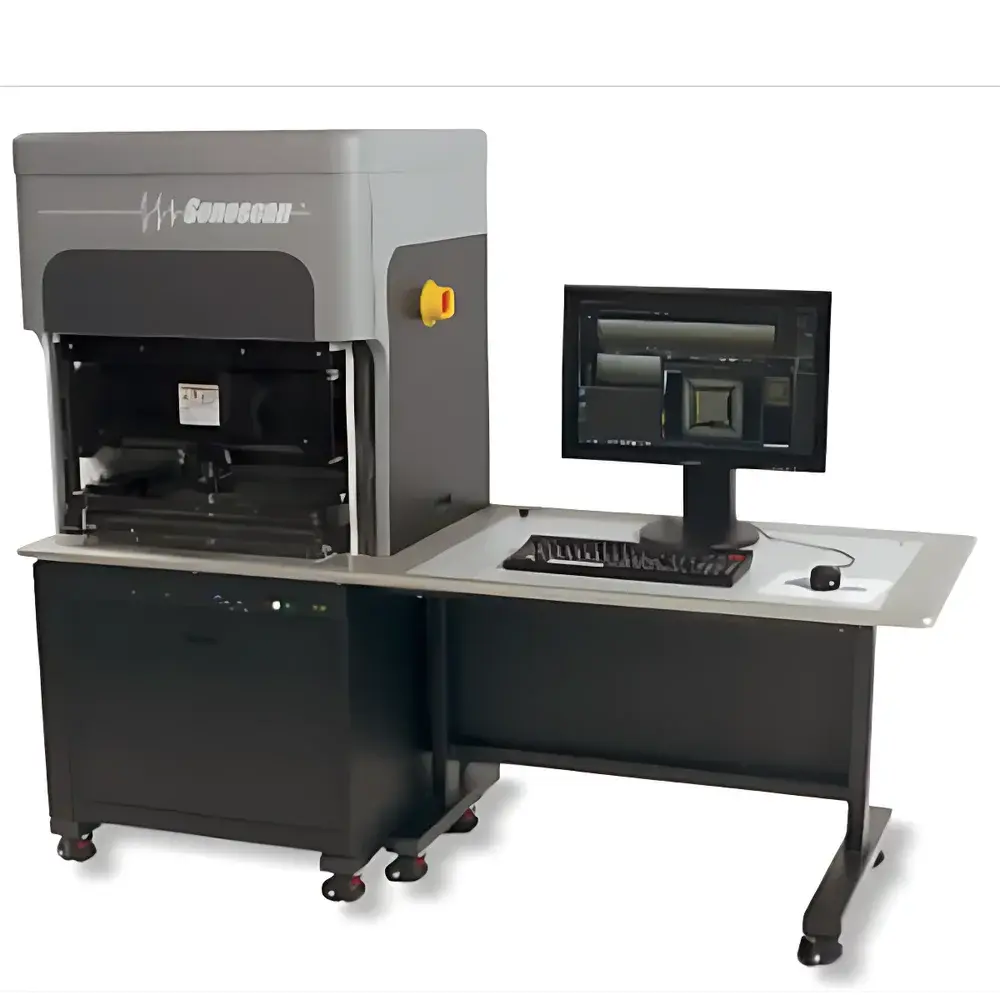
Sonoscan D9650 Scanning Acoustic Microscope (SAM)
| Brand | Sonoscan |
|---|---|
| Origin | USA |
| Model | D9650 |
| Application Domain | Aerospace, Semiconductor Packaging, Advanced Electronics Manufacturing, Power Electronics, MEMS, and Thin-Film Photovoltaics |
| Compliance | ASTM E1781, ISO 17845, IPC-J-STD-035, MIL-STD-883 Method 2030 |
| Detection Principle | Pulsed Ultrasound at Frequencies from 10 MHz to 230 MHz |
| Imaging Modes | C-scan, B-scan, A-scan, Through-Scan, Time-of-Flight (TOF), Phase-Sensitive (Phased Array Optional) |
Overview
The Sonoscan D9650 Scanning Acoustic Microscope (SAM) is a high-resolution, non-destructive imaging system engineered for subsurface defect detection and material interface analysis in advanced electronic packages, power devices, and aerospace-grade assemblies. Operating on the principle of pulse-echo ultrasonic time-of-flight measurement, the D9650 transmits focused acoustic energy—typically between 10 MHz and 230 MHz—into solid or layered materials and captures reflected echoes at acoustic impedance boundaries. Variations in echo amplitude, phase, and arrival time enable quantitative mapping of delaminations, voids, cracks, porosity, and bond integrity without physical sectioning or sample preparation. Its immersion-based scanning architecture ensures consistent coupling and thermal stability, critical for repeatable metrology in high-reliability manufacturing environments governed by AS9100, J-STD-035, and MIL-STD-883 Method 2030.
Key Features
- Multi-frequency transducer support (10–230 MHz) with automatic frequency switching and focal depth optimization for heterogeneous stack-ups.
- High-precision XYZ motion control with sub-micron positional repeatability (< ±0.5 µm) and programmable scan area up to 300 × 300 mm.
- Real-time C-scan imaging with adjustable gate windows, dynamic range compression, and echo polarity inversion for enhanced contrast of weak interfaces.
- Integrated through-scan (T-scan) and time-of-flight (TOF) analysis for thickness mapping and velocity profiling in multi-layer structures.
- Phase-sensitive acquisition mode (optional phased-array transducer) enabling coherent beamforming and improved signal-to-noise ratio in highly attenuating materials.
- Ruggedized industrial chassis with temperature-stabilized water bath, ESD-safe enclosure, and IP54-rated electronics compartment for cleanroom-compatible deployment.
Sample Compatibility & Compliance
The D9650 accommodates a broad spectrum of geometrically complex and compositionally diverse specimens—including molded ICs, stacked-die BGAs, flip-chip bonded wafers, TEC modules, power IGBTs on ceramic substrates, FRP composites, metal foams, ball bearing assemblies, and thin-film solar cells. Its immersion scanning method supports both rigid and compliant samples up to 50 mm in height and 3 kg in mass. All data acquisition and reporting workflows comply with industry standards for non-destructive evaluation: ASTM E1781 (Standard Practice for Ultrasonic Testing of Electronic Components), ISO 17845 (Ultrasonic inspection of microelectronic devices), IPC-J-STD-035 (Acoustic Microscopy Evaluation of Plastic Encapsulated Microcircuits), and MIL-STD-883 Method 2030 (Ultrasonic Inspection of Die Attach). Audit-ready metadata capture includes transducer ID, gain settings, gate parameters, water temperature, and operator credentials.
Software & Data Management
The D9650 operates under Sonoscan’s proprietary SAMView™ software platform, which provides full traceability per FDA 21 CFR Part 11 requirements—including electronic signatures, audit trails, and role-based access control. Image datasets are stored in vendor-neutral DICOM-SAM format with embedded EXIF-like metadata. Batch analysis tools support automated defect classification using threshold-based segmentation, size distribution histograms, and statistical process control (SPC) charting. Export options include TIFF, PNG, CSV, and XML for integration into LIMS, MES, and PLM systems. Software validation documentation (IQ/OQ/PQ protocols) is available upon request for GMP/GLP-regulated facilities.
Applications
- Detection of die attach voids and delamination in high-power SiC and GaN devices used in avionics and electric propulsion systems.
- Qualification of solder joint integrity and intermetallic formation in aerospace-grade PCB assemblies subjected to thermal cycling.
- Assessment of wafer-level bonding quality in MEMS inertial sensors and CMOS image sensor stacks.
- Failure analysis of LED die bonds in high-brightness lighting modules exposed to humidity and thermal stress.
- Characterization of adhesive bond lines and fiber-matrix debonding in carbon-fiber reinforced polymer (CFRP) structural components.
- Verification of ceramic-to-metal brazing in vacuum interrupter housings and RF filter substrates.
FAQ
What is the minimum detectable void size at 100 MHz in silicon?
Typical lateral resolution is ~15 µm; minimum resolvable void diameter in Si is approximately 25 µm under optimal coupling and SNR conditions.
Can the D9650 perform automated pass/fail inspection on production lines?
Yes—via custom script-driven acquisition and rule-based defect classification in SAMView™, with integration into PLC-controlled handling systems.
Is TOF-based thickness mapping supported for multi-layer ceramic capacitors (MLCCs)?
Yes—the system calculates layer thicknesses with ±0.5 µm accuracy using calibrated sound velocity values for common dielectric materials (e.g., BaTiO₃, Al₂O₃).
Does the system meet requirements for AS9100-certified suppliers?
Yes—hardware design, calibration traceability (NIST-traceable reference standards), and software audit trail functionality align with AS9100D Clause 8.5.2 on nonconforming output control.
Are transducers interchangeable between D9650 and earlier Sonoscan platforms?
Most legacy transducers (e.g., 50–230 MHz focusable models) are mechanically and electrically compatible; firmware updates may be required for full feature parity.
Related Products


