SOPTOP AWL Series Wafer Handling and Optical Defect Inspection System
| Brand | SOPTOP |
|---|---|
| Origin | Zhejiang, China |
| Manufacturer Type | Original Equipment Manufacturer (OEM) |
| Regional Classification | Domestic (China) |
| Model | AWL Series |
| Pricing | Upon Request |
| Primary Applications | Front-end & back-end wafer process monitoring, outgoing wafer quality control |
| Supported Wafer Diameters | 100 mm, 150 mm, 200 mm, 300 mm |
| Configurations | AWL046 (4″/6″), AWL068 (6″/8″), AWL812 (8″/12″) |
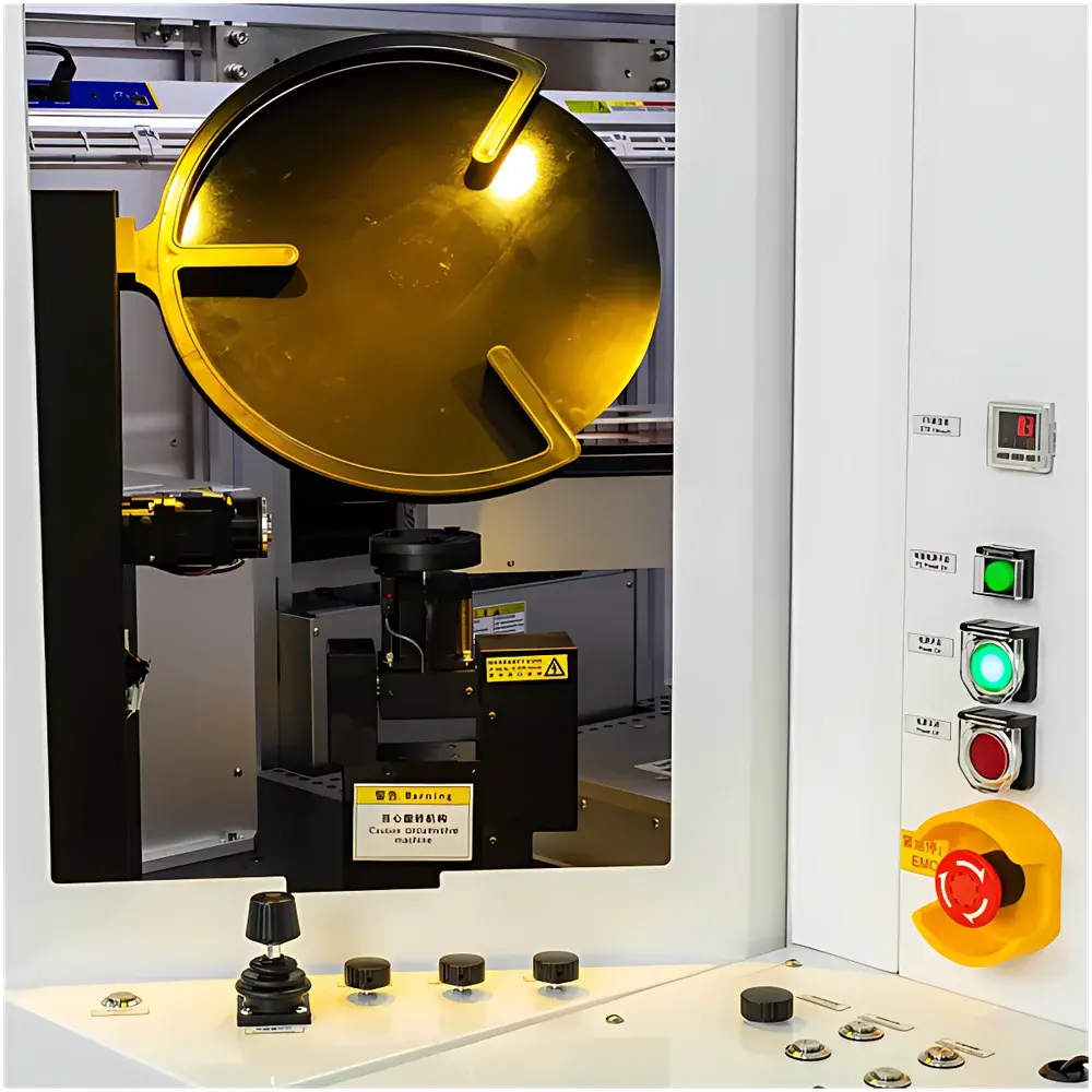
| Macro Inspection | 360° full-rotation stage with dual-side tilt (front-side max 70°, back-side 1 max 90°, back-side 2 max 160°) |
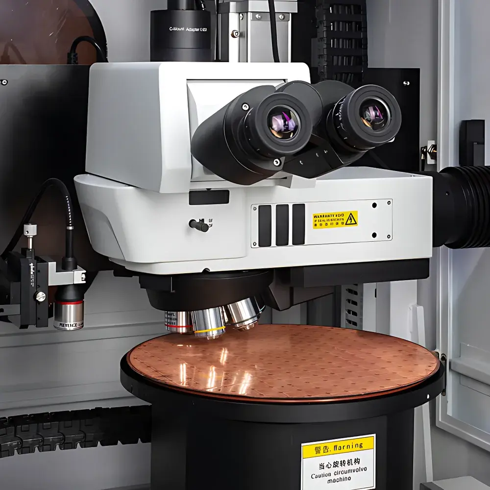
| Micro Inspection | Semi-apochromatic metallurgical objectives supporting brightfield, darkfield, DIC, and polarized light modes |
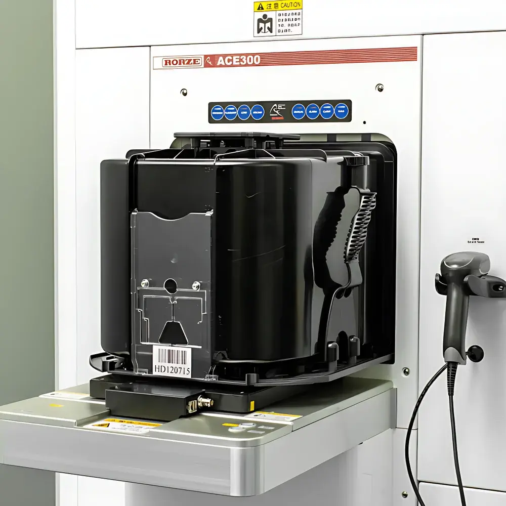
| Vacuum Chuck | Manual quick-release mechanism |
| Control System | Motorized precision stage with μm-level defect resolution |
Overview
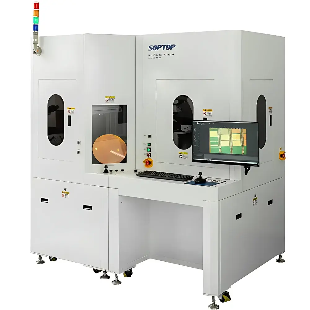
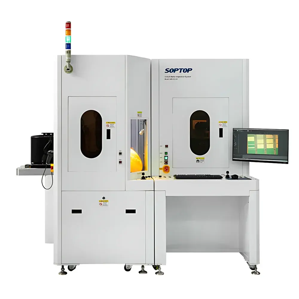
The SOPTOP AWL Series Wafer Handling and Optical Defect Inspection System is an integrated semiconductor metrology platform engineered for high-reliability, non-contact visual inspection across front-end fabrication and backend packaging workflows. Designed in accordance with industry-standard cleanroom compatibility requirements (ISO Class 5–7), the AWL system combines robust mechanical handling architecture with multi-modal optical imaging to support both macro-scale surface integrity assessment and micro-scale defect identification down to the micrometer level. Its core measurement principle relies on high-resolution reflected-light microscopy augmented by programmable illumination geometry, rotational kinematics, and controlled angular tilting—enabling comprehensive topographic evaluation of wafer frontside, backside, and bevel regions without physical contact or vacuum-induced stress deformation. The system operates as a standalone workstation or integrates into automated fab environments via SECS/GEM-compliant communication protocols.
Key Features
- Modular mechanical design accommodating multiple wafer diameters: AWL046 supports 100 mm and 150 mm wafers; AWL068 handles 150 mm and 200 mm substrates; AWL812 is optimized for 200 mm and 300 mm wafers—ensuring scalability across technology nodes from mature to advanced logic and memory processes.
- 360° continuous rotation stage with independent dual-axis tilt capability: frontside tilt up to ±70°, backside 1 tilt up to ±90°, and backside 2 tilt up to ±160°, enabling full circumferential edge inspection and oblique-angle defect visualization under variable incidence conditions.
- Motorized precision positioning system with sub-micron repeatability, synchronized with semi-apochromatic metallurgical objectives offering diffraction-limited resolution across brightfield, darkfield, differential interference contrast (DIC), and polarized light modalities.
- Ergonomic human-machine interface featuring a high-brightness LCD display showing real-time inspection sequence, active parameter set, stage coordinates, and lighting configuration—designed to minimize operator fatigue during extended shift cycles.
- Manual quick-release vacuum chuck with low-outgassing elastomer sealing, compliant with SEMI S2-0201 safety guidelines, reducing wafer loading/unloading time while maintaining surface cleanliness per ISO 14644-1 particle count thresholds.
Sample Compatibility & Compliance
The AWL Series supports silicon, silicon carbide (SiC), gallium nitride (GaN), and compound semiconductor wafers with thicknesses ranging from 100 µm to 1,000 µm. All models meet SEMI E10 standard specifications for equipment reliability and maintainability, and are compatible with common photomask reticle carriers and FOUP/SMIF load ports. The optical path is sealed against ambient particulate ingress, and the system’s mechanical structure conforms to SEMI S8-0701 vibration sensitivity limits. For regulated environments, audit trails, user access control, and electronic signature functionality can be enabled to align with FDA 21 CFR Part 11 and ISO/IEC 17025 documentation requirements.
Software & Data Management
The AWL system runs on a deterministic real-time operating system with embedded image acquisition firmware. Inspection recipes—including illumination profiles, focus maps, tilt sequences, and region-of-interest (ROI) definitions—are stored in encrypted XML format. Image metadata includes timestamp, operator ID, wafer ID (via optional barcode/RFID integration), magnification, and environmental sensor logs (temperature, humidity). Export formats include TIFF (16-bit), PNG, and CSV-based defect coordinate tables compatible with factory MES systems such as Applied Materials EnduraLink or PDF Solutions Exensio. Optional software modules support statistical process control (SPC) charting, defect clustering analysis, and automated pass/fail classification using configurable threshold rules—not AI-based classification—to ensure traceability and regulatory defensibility.
Applications
- Pre- and post-lithography surface inspection for pattern fidelity verification and resist residue detection.
- Post-CMP wafer evaluation for scratch, pit, and haze characterization in accordance with ASTM F2651 and SEMI MF1702 standards.
- Backgrinding and dicing tape inspection for voids, delamination, and particle adhesion prior to die separation.
- Final outgoing quality assurance for foundry and OSAT customers, supporting AQL sampling plans per ISO 2859-1 Level II.
- Process development lab use for root cause analysis of yield-limiting defects, including metal lift-off failures, etch residues, and contamination events.
FAQ
Does the AWL system support automatic defect classification?
No—it provides high-fidelity image capture and manual or rule-based defect flagging only. Automated classification requires external machine vision software validated separately under GMP/GLP frameworks.
Can the AWL series integrate with existing factory automation infrastructure?
Yes—via standard TCP/IP Ethernet with SECS/GEM protocol stack; custom OPC UA or Modbus TCP gateways are available upon request.
What is the maximum allowable wafer warpage for stable inspection?
Up to 50 µm total indicator reading (TIR) at 300 mm diameter, verified using calibrated interferometric reference wafers.
Is calibration traceable to national metrology institutes?
Yes—length scale calibration uses NIST-traceable step-height standards; intensity uniformity is verified per ISO 13660 Annex B.
How often does the system require preventive maintenance?
Every 1,000 operational hours or biannually—whichever occurs first—with documented service history stored locally and exportable for internal QA audits.


