SPECS Phoibos 190 ARPES System with UV and Soft X-ray Sources
| Brand | SPECS |
|---|---|
| Origin | Germany |
| Model | Phoibos 190 ARPES System |
| Energy Analyzer | ASTRAIOS 190 hemispherical analyzer with 2D-CMOS detector |
| Angular Resolution | <0.1° |
| Energy Resolution | <1.5 meV (with 2D-CMOS) |
| Acceptance Angle | ±30° |
| Vacuum Base Pressure | <1×10⁻¹⁰ mbar |
| Sample Stage | Closed-cycle 6-axis cryogenic manipulator (base temperature <7 K) |
| UV Source | UVS300 plasma discharge He lamp + TMM304 monochromator (HeI α/β, HeII lines |
| Soft X-ray Source | u-FOCUS 600 micro-focused monochromated Al/Ag/Cr anode (Rolan circle radius 600 mm |
| Detector | 1920×1200 pixel CMOS sensor, 160 fps frame rate, dynamic range >1×10⁶ cps, single-channel noise <0.002 cps |
| Software | SPECS Prodigy Suite (acquisition, real-time k-space mapping, Fermi surface reconstruction, GLP-compliant audit trail) |
Overview
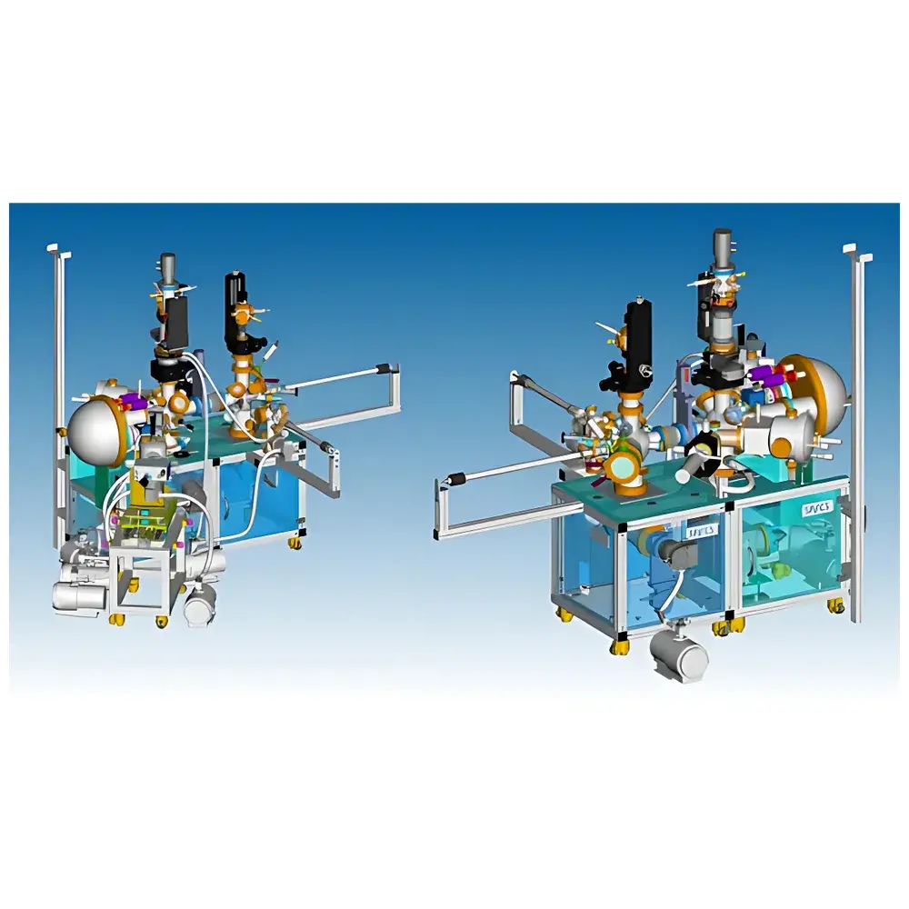
The SPECS Phoibos 190 ARPES System is a high-vacuum, ultra-high-resolution angle-resolved photoemission spectroscopy platform engineered for direct experimental determination of electronic band structure E(k) in crystalline solids. Based on the photoelectric effect, the system irradiates a single-crystal sample with tunable vacuum ultraviolet (VUV) or soft X-ray photons and measures the kinetic energy and emission angle of emitted photoelectrons with simultaneous high energy and angular fidelity. Unlike conventional XPS or UPS—where electron trajectories are integrated over solid angle—the Phoibos 190 implements momentum-resolved detection via a 190 mm radius ASTRAIOS hemispherical energy analyzer coupled to a low-noise, high-frame-rate 2D-CMOS detector. This architecture enables full two-dimensional acquisition of energy–angle (E–θ) distributions in a single exposure, which are then mapped onto crystal momentum space (kx, ky) using precise geometric calibration and known photon energy. The system operates under base pressures below 1×10⁻¹⁰ mbar to ensure surface integrity during measurement and supports both surface-sensitive UV-ARPES (using HeI/HeII lines) and bulk-probing SX-ARPES (using monochromated Al/Ag/Cr X-rays), making it suitable for interrogating topological surface states, interfacial charge transfer, superconducting gaps, and many-body renormalizations across diverse quantum materials.
Key Features
- ASTRAIOS 190 hemispherical energy analyzer with 150 mm mean radius, 40 mm working distance, and multi-mode lens optics (magnification, angular-resolving, transmission, and deflection modes)
- 1920×1200 pixel back-illuminated CMOS detector enabling parallel single-photon counting at >5000 counts per 40 ps time window, 160 fps frame rate, and dynamic range exceeding 1×10⁶ cps
- Closed-cycle 6-axis cryogenic manipulator with <7 K base temperature, sub-micron positioning repeatability, and in situ tilt/rotation/translation capabilities
- Dual excitation source configuration: UVS300 He plasma lamp + TMM304 monochromator (delivering HeI α at 21.22 eV, HeI β at 23.09 eV, and HeII at 40.81 eV; spectral resolution <2 meV; total flux >1×10¹⁶ ph/s/sr)
- u-FOCUS 600 micro-focused soft X-ray source with selectable Al (1486.6 eV), Ag (2984.3 eV), or Cr (5414.8 eV) anodes, 600 mm Roland circle geometry, and spot size down to 250 μm at 20 W power
- μ-metal shielded main analysis chamber with integrated flanges for analyzer, sources, viewports, ion pumps, and residual gas analyzers
- Vacuum interconnect compatibility with MBE, LEEM/PEEM, STM, and near-ambient pressure XPS chambers via standard CF-150/CF-200 ports
Sample Compatibility & Compliance
The Phoibos 190 accommodates conductive and semiconducting single crystals, thin films, heterostructures, and exfoliated 2D materials mounted on standard Omicron-style sample holders. Its ultra-high vacuum environment (<1×10⁻¹⁰ mbar) ensures minimal surface contamination during extended acquisition—critical for studying reactive surfaces such as cuprate superconductors or transition metal dichalcogenides. All hardware and software components comply with ISO 9001 quality management standards. The Prodigy control and data acquisition suite supports 21 CFR Part 11-compliant electronic signatures, audit trails, and user-access-level permissions, meeting GLP/GMP requirements for regulated R&D environments. System calibration protocols adhere to ASTM E1901 (standard guide for photoelectron spectroscopy) and ISO 18118 (surface chemical analysis — XPS — terminology and conventions).
Software & Data Management
SPECS Prodigy is a modular, Python-based software platform providing end-to-end workflow integration—from instrument control and real-time k-space visualization to advanced post-processing. Key modules include: (1) Auto-calibration routines for energy and angular dispersion using reference spectra; (2) Fermi surface reconstruction tools with k∥ vector interpolation and momentum-space unfolding; (3) Band fitting algorithms based on Lorentzian/Gaussian deconvolution and maximum entropy methods; (4) Batch processing pipelines supporting HDF5-based data storage, metadata embedding (sample ID, temperature, photon energy, polarization), and FAIR-compliant export. Raw datasets are stored with timestamped acquisition logs, hardware state snapshots, and detector gain/offset records—enabling full traceability for peer-reviewed publication or regulatory submission.
Applications
This system delivers quantitative E(k) maps essential for fundamental research in condensed matter physics and quantum materials science. It is routinely deployed to characterize: (1) Topological insulators (e.g., Bi₂Se₃, Sb₂Te₃), resolving spin-momentum locked surface Dirac cones; (2) High-Tc cuprates and iron-based superconductors, identifying nodal gap structures and pseudogap evolution; (3) Twisted bilayer graphene and moiré heterostructures, mapping flat bands and correlated insulating states; (4) Charge density wave (CDW) and spin density wave (SDW) systems, tracking nesting vectors and order parameter symmetry; (5) Catalytic interfaces and oxide heterojunctions, probing band alignment and interfacial charge transfer via SX-ARPES depth profiling. Its dual UV/SX capability bridges surface-limited and bulk-sensitive regimes—enabling correlative studies across length scales inaccessible to conventional PES.
FAQ
What distinguishes UV-ARPES from SX-ARPES in this system?
UV-ARPES (21–41 eV) provides superior energy and momentum resolution for surface-state mapping, while SX-ARPES (1.5–5.4 keV) increases inelastic mean free path by ~5–10×, enabling bulk-sensitive band structure measurements and interface-selective probing in buried heterostructures.
Can the system perform spin-resolved ARPES?
Spin resolution is not natively integrated but can be added via optional Mott or VLEED spin detectors compatible with the Phoibos 190’s flange layout and UHV infrastructure.
Is in situ sample preparation supported?
Yes—the system includes dedicated preparation and load-lock chambers equipped with LEED optics, e-beam evaporators, sputter guns, and resistive heating stages, enabling atomic-layer cleaning, epitaxial growth, and dosing—all within the same UHV environment.
How is energy calibration performed?
Calibration uses Au 4f7/2 (84.0 eV) and Ag 3d5/2 (368.3 eV) reference spectra acquired under identical lens and pass-energy conditions; automated routines correct for work function drift and analyzer nonlinearity.
What level of technical support does SPECS provide post-installation?
SPECS offers on-site commissioning, operator training, annual preventive maintenance, remote diagnostics, and access to application scientists specializing in quantum materials characterization workflows.
Related Products
")
")