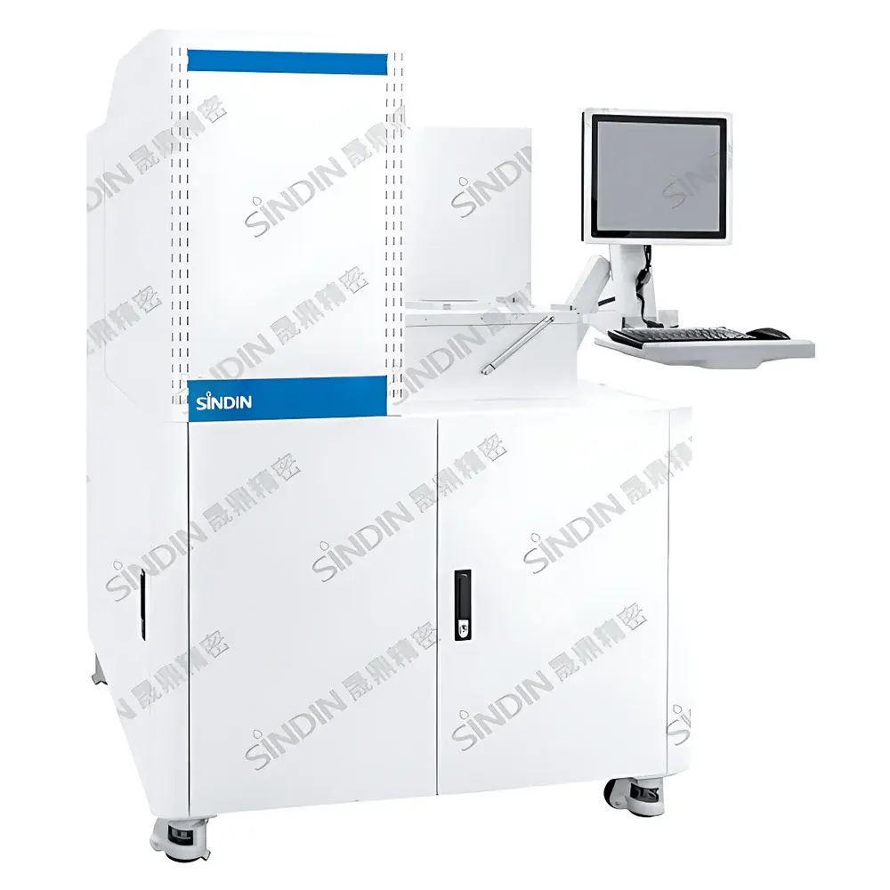
ST-2100MW Sindin Benchtop Plasma Resist Stripper for Semiconductor Wafers
| Brand | Sindin |
|---|---|
| Model | ST-2100MW |
| Origin | Guangdong, China |
| Manufacturer Type | Original Equipment Manufacturer (OEM) |
| Regional Classification | Domestic (PRC) |
| Pricing | Available Upon Request |
Overview
The ST-2100MW is a compact, benchtop plasma resist stripper engineered specifically for R&D, pilot-line processing, and low-volume fabrication of silicon, compound semiconductor, and MEMS wafers up to 200 mm (8-inch) diameter. It utilizes reactive ion etching (RIE) principles with dual-frequency capacitively coupled plasma (CCP) excitation—typically 13.56 MHz for ion energy control and 380 kHz or 2 MHz for ion flux modulation—to achieve highly anisotropic, residue-free photoresist removal while minimizing substrate damage and sidewall undercut. Unlike wet chemical stripping, this dry process eliminates solvent disposal concerns, reduces particle generation, and enables precise selectivity tuning via gas chemistry (e.g., O₂, CF₄/O₂, SF₆/O₂ mixtures), making it ideal for post-lithography, post-etch residue cleaning, and hard mask stripping in advanced node development.
Key Features
- Benchtop footprint (W × D × H ≈ 650 × 600 × 550 mm) optimized for cleanroom integration in Class 100–1000 environments
- Stainless-steel vacuum chamber with quartz viewing port and integrated RF shielding for electromagnetic compatibility
- Dual RF generator system (13.56 MHz + low-frequency source) with independent impedance matching networks for process stability across varying load conditions
- Programmable process controller supporting up to 99 multi-step recipes, each with adjustable RF power (0–300 W), pressure (1–100 mTorr), gas flow rates (0–200 sccm per channel), and step duration (0.1–9999 s)
- Integrated base pressure ≤5 × 10⁻⁶ Torr (with turbomolecular pump), ultimate process pressure range: 5–50 mTorr
- Wafer handling: Manual loading/unloading with electrostatic chuck (ESC) or mechanical clamping; compatible with standard wafer carriers (FOUP/SMIF optional via retrofit)
- Real-time monitoring of chamber pressure, forward/reflected RF power, and gas flow via digital display and RS485/Ethernet interface
Sample Compatibility & Compliance
The ST-2100MW accommodates bare and patterned wafers from 100 mm (4-inch) to 200 mm (8-inch), including Si, SiC, GaN, SOI, and glass substrates. It supports both positive and negative tone resists (e.g., AZ® series, Shipley® S18xx, TOK® TMMR), as well as metal hard masks (TiN, TaN) and dielectric anti-reflective coatings (BARC). The system conforms to IEC 61000-6-2 (immunity) and IEC 61000-6-4 (emission) standards. Vacuum and gas delivery components meet SEMI F57 (vacuum fittings) and SEMI F21 (gas purity) specifications. Optional documentation packages support GLP/GMP-aligned process validation, including IQ/OQ protocols and traceable calibration records for pressure gauges and mass flow controllers.
Software & Data Management
Equipped with Sindin’s proprietary PlasmaControl™ v3.2 software, the ST-2100MW provides local touchscreen operation and remote PC-based supervision via TCP/IP. All process parameters, timestamps, alarm logs, and real-time sensor traces are stored in SQLite databases with configurable retention policies. Audit trail functionality complies with FDA 21 CFR Part 11 requirements when configured with user role management (Admin/Operator/Viewer), electronic signatures, and immutable log archiving. Export formats include CSV, PDF reports, and XML for integration into MES platforms such as Siemens Opcenter Execution (formerly Camstar) or Applied Materials EnduraConnect.
Applications
- Photoresist stripping after lithographic patterning or ion implantation
- Removal of residual polymers and etch byproducts following dry etch processes (e.g., SiO₂, SiNₓ, metal etch)
- Surface activation and cleaning prior to bonding, deposition, or metrology
- Development of low-damage stripping chemistries for EUV resists and ultra-thin films
- Process qualification and failure analysis in university cleanrooms, foundry NPI labs, and packaging R&D centers
FAQ
What wafer sizes does the ST-2100MW support?
Standard configuration supports 100 mm, 150 mm, and 200 mm wafers. Custom chucks for non-standard diameters or irregular substrates (e.g., diced dies, LED wafers) are available upon request.
Is ozone or NOx generation mitigated in the exhaust system?
Yes—the system includes an integrated catalytic ozone destruct unit and optional scrubber module compliant with local environmental regulations (e.g., EPA Method 204, ISO 14644-8 particle classification for abatement effluent).
Can the ST-2100MW be integrated into an automated cluster tool environment?
While primarily designed as a standalone tool, it supports SECS/GEM communication protocol and can be interfaced with factory host systems via Ethernet/IP or Modbus TCP for semi-automated batch handling.
Does Sindin provide installation qualification (IQ) and operational qualification (OQ) documentation?
Yes—comprehensive IQ/OQ templates aligned with ISO/IEC 17025 and SEMI E10 guidelines are included. On-site qualification support and third-party certification coordination are available as value-added services.


