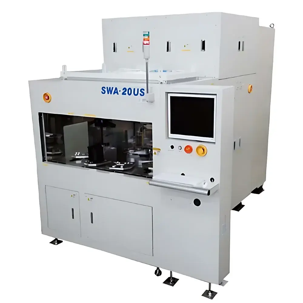
Sumitomo SAW-20US Laser Rapid Thermal Annealing (RTA) System
| Brand | Sumitomo |
|---|---|
| Origin | Japan |
| Manufacturer Type | Authorized Distributor |
| Origin Category | Imported |
| Model | SAW-20US |
| Price Range | USD 1,050,000 – 1,210,000 |
Overview
The Sumitomo SAW-20US Laser Rapid Thermal Annealing (RTA) System is a high-precision, localized thermal processing instrument engineered for advanced semiconductor fabrication and R&D laboratories. Unlike conventional furnace-based annealing, the SAW-20US employs high-power, wavelength-stabilized diode-pumped solid-state (DPSS) lasers to deliver spatially confined, millisecond-scale thermal pulses directly onto wafer surfaces. This enables ultra-fast heating (>100 °C/ms) and controlled cooling profiles—critical for minimizing dopant diffusion, activating ultra-shallow junctions, repairing ion-implantation damage, and crystallizing amorphous silicon layers without bulk substrate overheating. The system operates under high-vacuum or inert-gas ambient conditions (N2, Ar), supporting process repeatability compliant with semiconductor manufacturing requirements.
Key Features
- Laser source: Dual-wavelength (e.g., 532 nm + 1064 nm) DPSS laser modules with real-time power stabilization and beam homogenization optics for uniform energy distribution across target areas.
- Thermal control: Closed-loop pyrometry feedback with sub-millisecond response time, enabling temperature accuracy of ±1.5 °C within 500–1300 °C range (calibrated against Si bandgap reference).
- Wafer handling: Fully automated 200 mm (8-inch) wafer loading/unloading via vacuum chucks; optional upgrade path to 300 mm compatibility with reticle alignment stage.
- Process chamber: Stainless-steel UHV-compatible chamber (base pressure <5×10⁻⁷ Torr), integrated with residual gas analyzer (RGA) and mass flow controllers for precise ambient gas composition management.
- System architecture: Modular design compliant with SEMI S2/S8 safety standards; CE-marked; equipped with interlocked access doors and Class 4 laser enclosure per IEC 60825-1.
Sample Compatibility & Compliance
The SAW-20US accommodates standard semiconductor substrates including Si, SiC, GaN, Ge, SOI, and compound semiconductor wafers up to 200 mm in diameter and 0.5–1.5 mm thickness. It supports patterned and unpatterned wafers with backside metallization or dielectric coatings. Process recipes are validated per ASTM F1929 (laser-induced thermal processing characterization) and aligned with JEDEC JESD22-A108 for thermal stress reliability testing. All operational logs—including laser energy, chamber pressure, pyrometer readings, and gas flows—are timestamped and stored with audit-trail capability, satisfying GLP/GMP documentation requirements and FDA 21 CFR Part 11 electronic record integrity criteria.
Software & Data Management
Control and monitoring are executed via Sumitomo’s proprietary RTA-Manager™ software suite, running on a deterministic real-time OS. The interface provides full recipe scripting (Python API support), multi-zone thermal profiling, and synchronized data acquisition at up to 10 kHz sampling rate. Process data—including thermal transients, laser pulse timing, and environmental parameters—is exported in HDF5 format for traceable integration into MES platforms (e.g., Applied Materials EnduraConnect, Tokyo Electron TELVision). Built-in calibration wizards support NIST-traceable pyrometer recalibration and laser energy meter validation. Software versioning, user role-based access control (RBAC), and electronic signature functionality ensure compliance with ISO 9001 and IATF 16949 quality management frameworks.
Applications
- Activation annealing of ultra-low-energy ion implants (e.g., B, P, As at energies <1 keV) for FinFET and nanosheet transistor nodes.
- Recrystallization of amorphous silicon layers in TFT-LCD and micro-LED backplane fabrication.
- Ohmic contact formation on wide-bandgap semiconductors (SiC, GaN) without interfacial reaction layer growth.
- Low-temperature annealing of metal-oxide thin films (e.g., IGZO, HfO2) for gate stack optimization in flexible electronics.
- Research-scale thermal budget studies for novel 2D material integration (MoS2, WS2) on Si or sapphire substrates.
FAQ
What wafer sizes does the SAW-20US support natively?
The system is configured for 200 mm wafers; 300 mm capability requires optional mechanical and optical upgrades, including extended beam delivery and larger vacuum chuck assembly.
Is the laser wavelength tunable?
No—the SAW-20US uses fixed-wavelength DPSS lasers optimized for absorption depth matching in common semiconductor materials; wavelength selection is determined during system configuration based on primary application targets.
Can the system integrate with factory automation protocols?
Yes—it supports SECS/GEM communication over TCP/IP and provides SEMI E30/E37-compliant message sets for host equipment integration and remote job dispatch.
Does it meet cleanroom compatibility requirements?
Yes—the system meets ISO Class 5 particulate limits when operated in Class 100/ISO 5 environments; all internal materials comply with SEMI F57 outgassing specifications.
What maintenance intervals are recommended?
Laser source alignment verification every 500 hours; pyrometer calibration annually or after 2000 thermal cycles; vacuum pump oil change every 3000 operating hours—detailed schedules are embedded in the maintenance module of RTA-Manager™.


