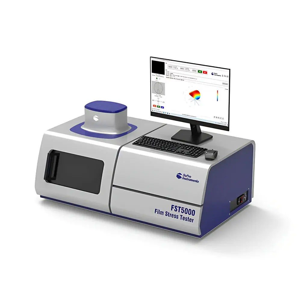
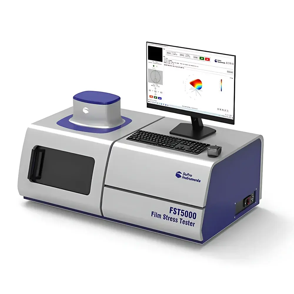
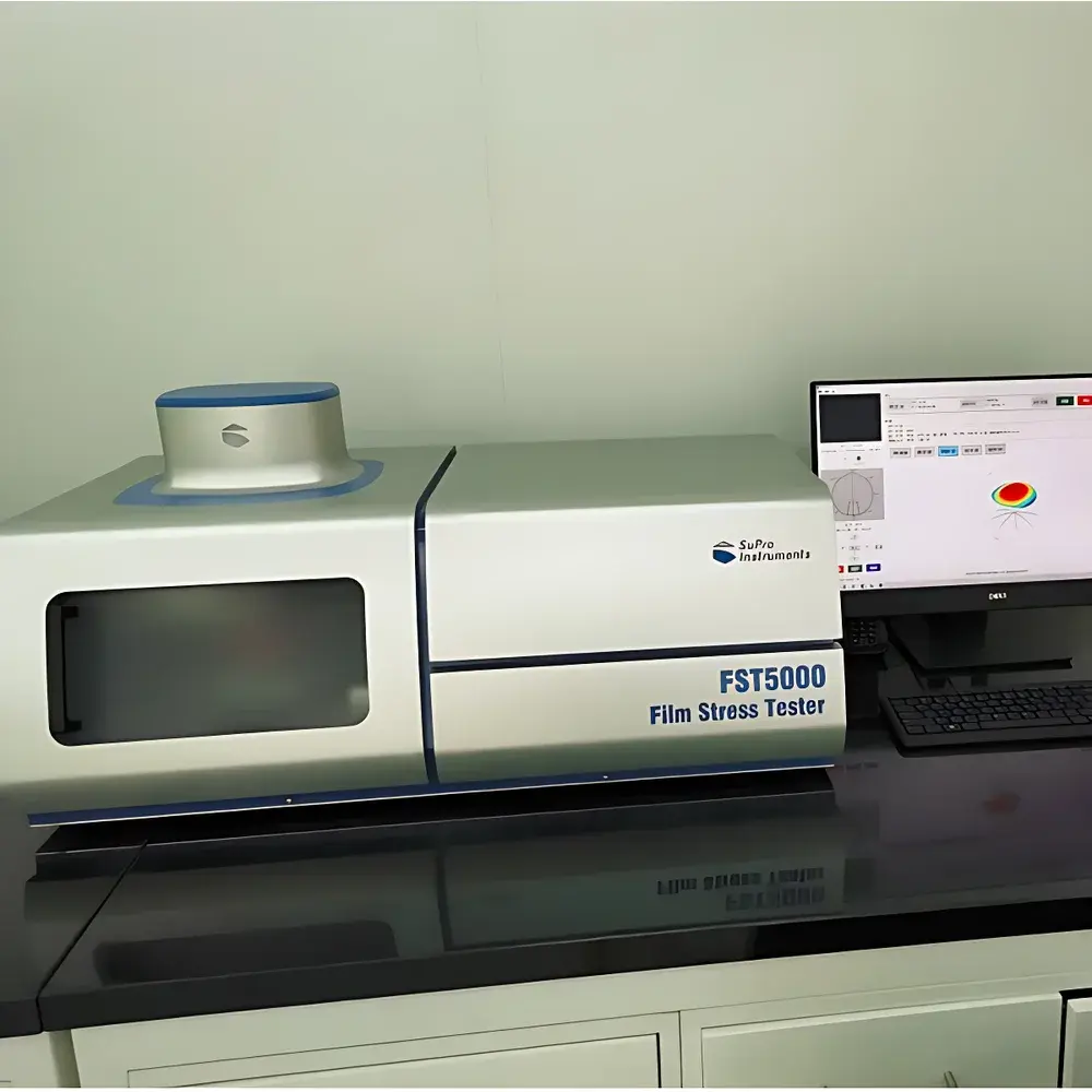
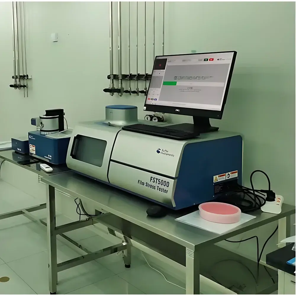
SuPro FST 5000 Thin Film Stress Tester
| Brand | SuPro Instruments |
|---|---|
| Origin | Guangdong, China |
| Manufacturer Type | Direct Manufacturer |
| Product Origin | Domestic (China) |
| Model | FST 5000 |
| Price | USD 84,000 (approx.) |
| Stress Measurement Range | 1–10,000 MPa (tensile or compressive) |
| Measurement Technology | Dual-Wavelength Laser Scanning |
| Operating Temperature | Ambient (20–25 °C) |
Overview
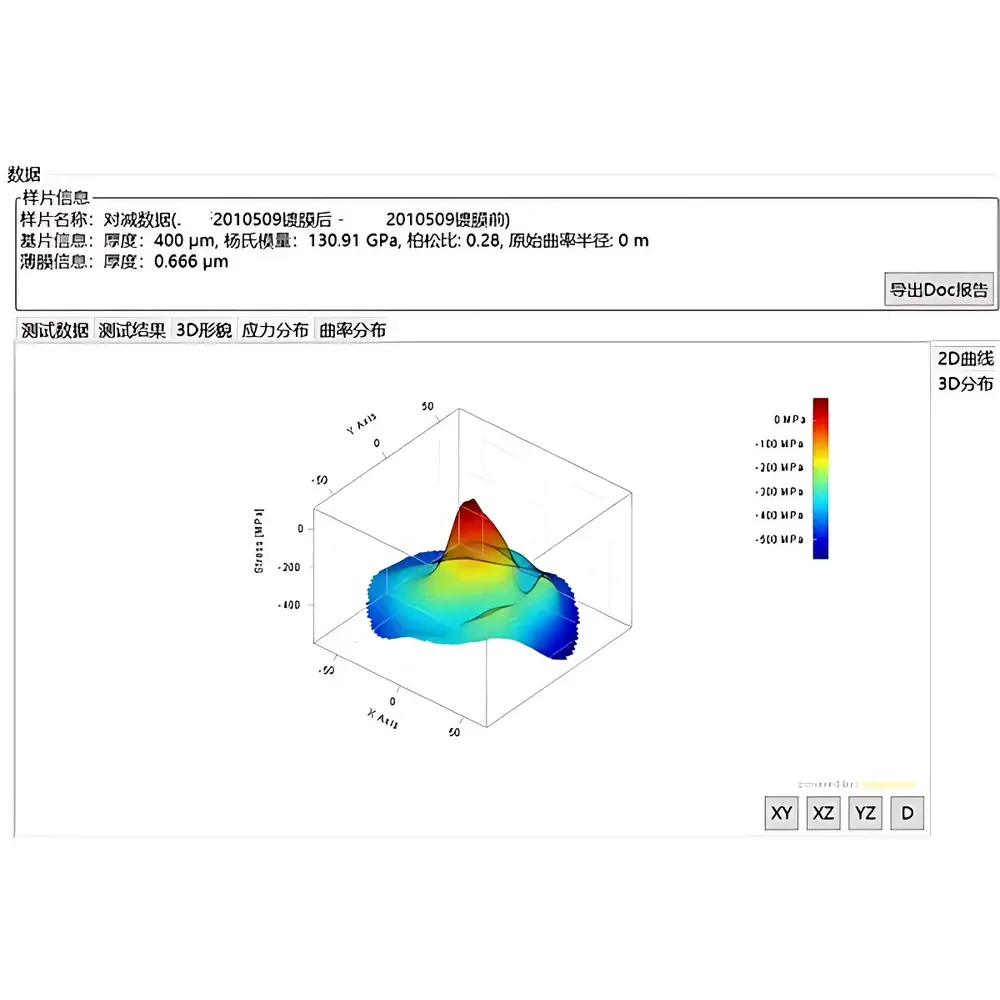
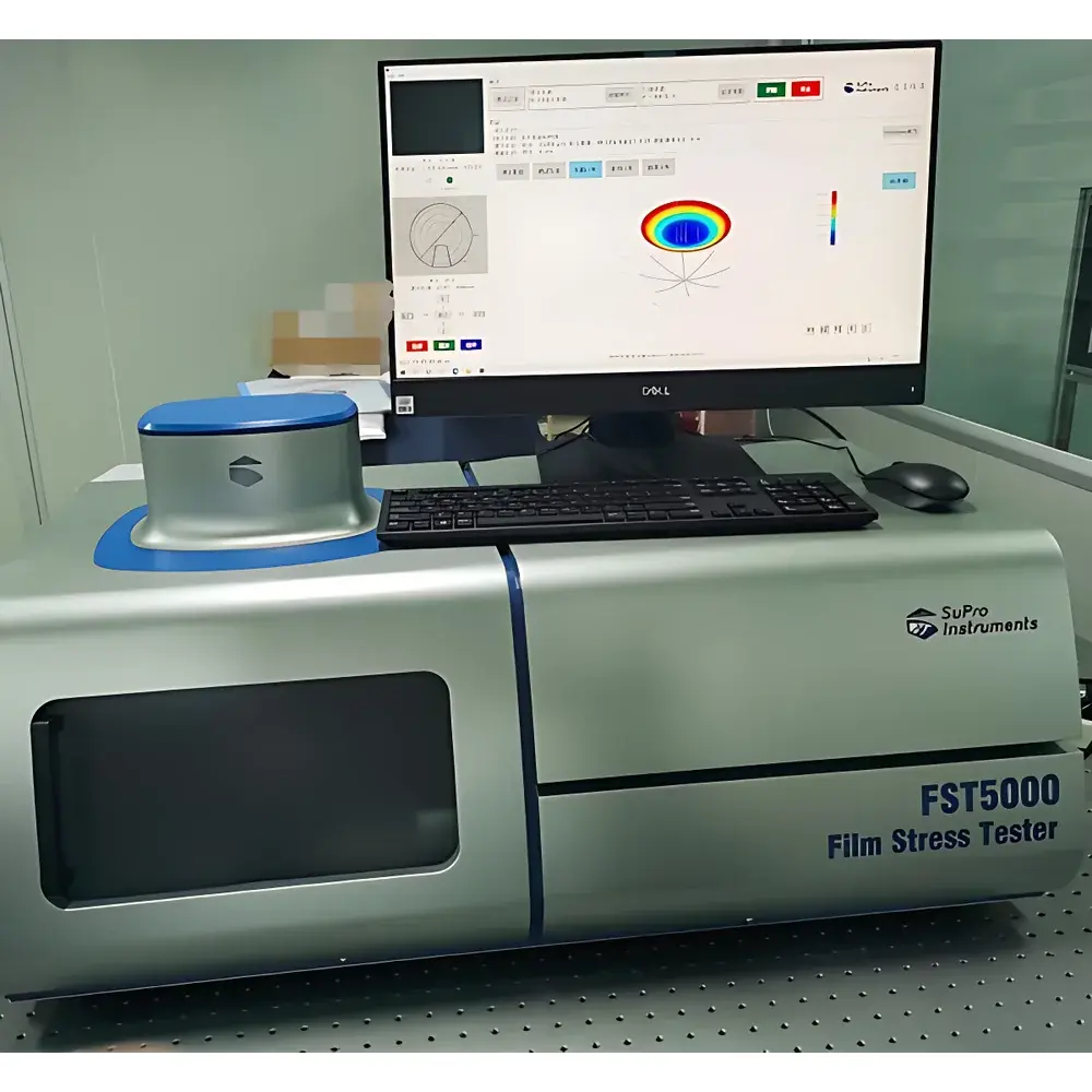
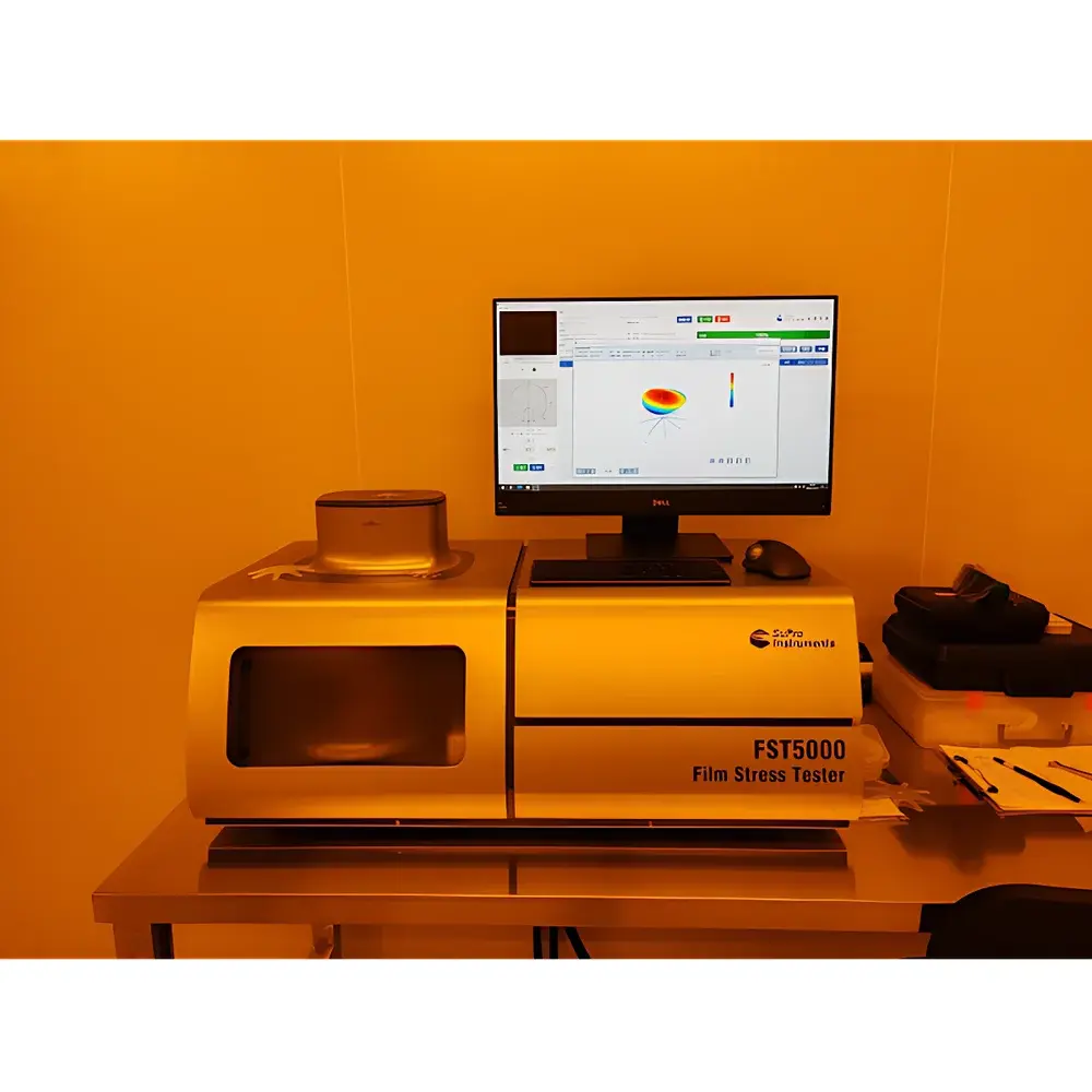
The SuPro FST 5000 Thin Film Stress Tester is an engineered metrology system designed for non-contact, high-precision quantification of residual mechanical stress in thin films deposited on rigid substrates—primarily silicon wafers, fused silica, sapphire, and other optically compatible planar substrates used in semiconductor fabrication, MEMS development, and optical coating processes. It operates on the well-established Stoney equation, which relates substrate curvature change (Δκ) to film stress (σf) via substrate modulus (Es), Poisson’s ratio (νs), and film/substrate thickness ratio (tf/ts). The FST 5000 implements this principle through dual-wavelength laser scanning interferometry, enabling simultaneous acquisition of surface topography and differential curvature across the full wafer diameter (up to 200 mm standard; configurable for 300 mm). Unlike single-point profilometers or manual curvature gauges, the FST 5000 delivers spatially resolved stress maps with sub-micrometer lateral resolution and nanometer-level vertical repeatability, supporting both front-side and back-side measurement configurations.
Key Features
- Dual-wavelength laser scanning architecture: Utilizes two stabilized HeNe lasers (632.8 nm and 543.5 nm) to suppress environmental drift and enhance signal-to-noise ratio during curvature differentiation.
- Full-wafer curvature profiling: Measures bow (sagitta), radius of curvature (RoC), and local curvature gradients across diameters up to 300 mm with ≤ ±0.5 m⁻¹ uncertainty in curvature determination.
- Stoney-based stress calculation engine: Integrates user-defined material constants (Es, νs, ts) and measured film thickness (tf) to compute in-plane biaxial stress distribution (MPa) with traceable uncertainty propagation.
- Automated alignment & calibration: Includes motorized XYZ stage with integrated fiducial detection for rapid centering and tilt compensation—critical for high-aspect-ratio or patterned wafers.
- Robust thermal management: Passive stabilization design ensures measurement stability within ±0.1 °C over 4-hour continuous operation at ambient lab conditions (20–25 °C, <50% RH).
- CE-compliant safety architecture: Fully enclosed laser path with interlocked access doors and Class 1 laser certification per IEC 60825-1:2014.
Sample Compatibility & Compliance
The FST 5000 supports flat, rigid substrates with optical quality surfaces and minimal surface roughness (Ra < 5 nm). Compatible sample types include bare silicon wafers (100, 111), SOI, GaAs, InP, quartz, BK7 glass, and metal-coated substrates (e.g., TiN, Al, Cr) where film thickness exceeds 10 nm. Substrate thickness range: 200–1000 µm. The instrument conforms to ISO 9001:2015 manufacturing standards and meets essential requirements of the EU Machinery Directive 2006/42/EC and Electromagnetic Compatibility Directive 2014/30/EU. While not FDA-registered, its data output format and audit trail capabilities support alignment with GLP and GMP environments when integrated into validated laboratory workflows per ASTM F394-22 (Standard Practice for Measuring Residual Stress in Thin Films Using the Wafer Curvature Method).
Software & Data Management
The FST 5000 is operated via SuPro StressView™ v4.2 software, a Windows-based application with role-based user accounts, electronic signature support, and full 21 CFR Part 11 compliance options (audit trail logging, data integrity controls, and secure export). Raw curvature maps are stored in HDF5 format with embedded metadata (timestamp, operator ID, calibration ID, environmental logs). Stress profiles can be exported as CSV, ASCII, or image (TIFF/PNG) with customizable color scales and contour overlays. Batch processing mode enables unattended analysis of multi-wafer lots, with pass/fail thresholds configurable per zone (center, edge, quadrant). All software updates are delivered via encrypted firmware packages with SHA-256 verification.
Applications
- Semiconductor process development: Quantifying stress evolution during PECVD SiNx, ALD Al2O3, sputtered TiW, and e-beam evaporated Au layers—enabling correlation with deposition parameters (power, pressure, temperature).
- MEMS reliability assessment: Monitoring stress-induced warpage in released cantilevers, diaphragms, and resonators pre- and post-packaging.
- Optical coating QC: Verifying low-stress conditions in anti-reflective (AR), high-reflective (HR), and dichroic stacks to prevent delamination or wavefront distortion.
- Advanced packaging R&D: Characterizing stress transfer at Cu/low-k interfaces in 2.5D/3D IC integration schemes.
- Academic thin-film research: Supporting studies on stress relaxation kinetics, thermal mismatch modeling, and epitaxial strain engineering.
FAQ
What substrates are supported by the FST 5000?
Silicon (100/111), SOI, quartz, sapphire, fused silica, and polished metal-coated wafers—provided surface roughness is below 5 nm Ra and thickness falls between 200–1000 µm.
Does the system require vacuum or controlled atmosphere?
No. The FST 5000 operates exclusively at ambient atmospheric conditions and does not integrate vacuum chambers or gas purging.
Can it measure stress in multilayer stacks?
Yes—when combined with independent film thickness measurements (e.g., ellipsometry or XRR), the Stoney model can be extended using superposition methods for bilayer or trilayer systems.
Is third-party calibration available?
Yes. NIST-traceable curvature reference standards (certified radii: 10 m, 50 m, 200 m) are offered by SuPro’s metrology service division, with annual recalibration recommended per ISO/IEC 17025 guidelines.
How is data integrity ensured for regulated environments?
StressView™ supports optional 21 CFR Part 11 modules including electronic signatures, immutable audit trails, and permission-controlled data export—fully deployable in FDA-audited cleanroom labs.


