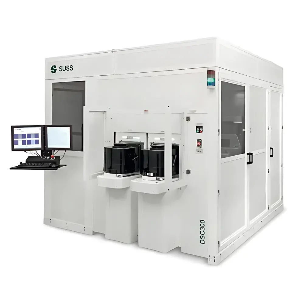
SUSS DSC300 Gen3 Projection Scanning Stepper
| Brand | SUSS |
|---|---|
| Origin | Germany |
| Model | DSC300 Gen3 |
| Wafer Size Support | 300 mm (optional 200 mm) |
| Resolution | 2 µm (line/space) |
| Overlay Accuracy | ≤1.0 µm |
| Depth of Focus (DOF) | High (NA-tunable) |
| Substrate Compatibility | Si, glass, SiC |
| Max. Warp Tolerance | 2 mm bow |
| Optical System | Wynne-Dyson broadband imaging optics |
| Exposure Source | Broadband UV (g-, h-, i-line compatible) |
| Operation Mode | Full-field projection + continuous scanning |
| Automation Level | Fully automated platform |
Overview
The SUSS DSC300 Gen3 Projection Scanning Stepper is a high-throughput, full-field photolithography platform engineered for advanced packaging applications in semiconductor manufacturing. Unlike conventional step-and-repeat steppers or mask aligners, the DSC300 Gen3 employs a proprietary continuous scanning exposure method combined with a full-field UV illumination system—enabling seamless, non-overlapping pattern transfer across the entire wafer surface. This architecture eliminates stitching errors, field-edge dose non-uniformity, and mechanical stepping artifacts commonly associated with traditional stepper systems. The system operates on a 1× magnification projection principle using a Wynne-Dyson optical design, optimized for broadband UV wavelengths (g-, h-, and i-line), delivering high-fidelity image fidelity, excellent depth of focus (DOF), and superior critical dimension (CD) uniformity. Designed specifically for wafer-level packaging (WLP), fan-out wafer-level packaging (FOWLP), and 2.5D/3D heterogeneous integration processes, the DSC300 Gen3 supports both high-resolution patterning (down to 2 µm L/S) and thick resist processing—making it suitable for redistribution layer (RDL), bump, and via patterning steps where overlay accuracy, process stability, and cost-of-ownership are critical.
Key Features
- Wynne-Dyson broadband optical system with tunable numerical aperture (NA) for balanced resolution and DOF optimization
- Overlay accuracy ≤1.0 µm (3σ) enabled by high-stability optical alignment, off-axis infrared (IR) alignment capability, and real-time wafer offset compensation
- Continuous scanning exposure mode ensures defect-free, stitch-free imaging—eliminating field boundary effects and dose variation across large-area patterns
- Full compatibility with 300 mm wafers (200 mm optional); accommodates substrates including silicon, fused silica, and silicon carbide
- Robust substrate handling architecture supporting up to 2 mm bow (static warp), essential for warped advanced packaging substrates
- Modular optical configuration: interchangeable filters and NA settings enable adaptation to diverse resist thicknesses and feature sizes—from fine-pitch RDL layers to thick photoresist for plating and etch applications
- Fully automated platform with integrated load ports, robotic wafer handling, and recipe-driven operation compliant with SEMI E47.1 standards
Sample Compatibility & Compliance
The DSC300 Gen3 is validated for use with standard positive and negative tone photoresists (e.g., AZ®, Shipley®, Tokyo Ohka Kogyo resists) and supports both contact and proximity-mode compatible resist formulations. Its broadband UV source allows process flexibility across g-line (436 nm), h-line (405 nm), and i-line (365 nm) exposure spectra—ensuring compatibility with industry-standard resist sensitivity profiles. The system meets ISO 14644-1 Class 5 cleanroom requirements when installed with appropriate environmental enclosures. All motion control, alignment, and exposure subsystems are designed to comply with IEC 61000-6-2 (EMC immunity) and IEC 61000-6-4 (EMC emissions) standards. Data logging, user access control, and audit trail functionality support GLP/GMP-aligned environments and can be configured to meet FDA 21 CFR Part 11 requirements when integrated with SUSS’s certified Process Control Software (PCS).
Software & Data Management
The DSC300 Gen3 runs on SUSS’s proprietary Process Control Software (PCS), a Windows-based, multi-user interface offering full recipe management, real-time exposure monitoring, and comprehensive process traceability. PCS supports hierarchical recipe structures, parameter versioning, and electronic signature workflows. All alignment data, exposure logs, stage positioning records, and environmental sensor readings (temperature, humidity, vibration) are timestamped and stored in an encrypted SQLite database. Export functions include CSV and XML formats for SPC analysis and MES integration via SECS/GEM protocol (SEMI E30/E37 compliant). Optional remote diagnostics and predictive maintenance modules leverage embedded sensor telemetry for uptime optimization and proactive service scheduling.
Applications
- Redistribution Layer (RDL) patterning for fan-out wafer-level packaging (FOWLP)
- Microbump and copper pillar formation in 2.5D/3D interposer and TSV integration
- Thick resist patterning for electroplating, deep etch, and solder mask applications
- MEMS packaging lithography requiring high DOF and low thermal drift
- Compound semiconductor substrate processing (e.g., GaN-on-SiC, Si photonics wafers)
- High-volume prototyping and pilot-line production of advanced packaging interconnects
FAQ
What exposure wavelengths does the DSC300 Gen3 support?
The system uses a broadband UV source with selectable g-, h-, and i-line spectral filtering, enabling compatibility with standard i-line resists as well as legacy g/h-line processes.
Can the DSC300 Gen3 handle warped or non-planar substrates?
Yes—it supports static bow up to 2 mm and integrates dynamic focus compensation during scanning to maintain consistent focus across warped surfaces.
Is the system compatible with existing fab automation infrastructure?
Yes—equipped with SECS/GEM interface, E84 carrier handling compliance, and standard 300 mm FOUP load ports per SEMI E47.1 and E157 specifications.
How is overlay accuracy maintained across multiple exposure fields?
Through real-time wafer offset correction using IR alignment marks, proprietary beam-steering optics, and thermal drift compensation algorithms embedded in the PCS alignment engine.
Does SUSS provide process qualification support for new resist or substrate combinations?
Yes—SUSS Applications Engineering offers joint process development services, including DOE-based optical calibration, resist characterization, and CD uniformity mapping per ASTM F2190 and ISO 13121 standards.


