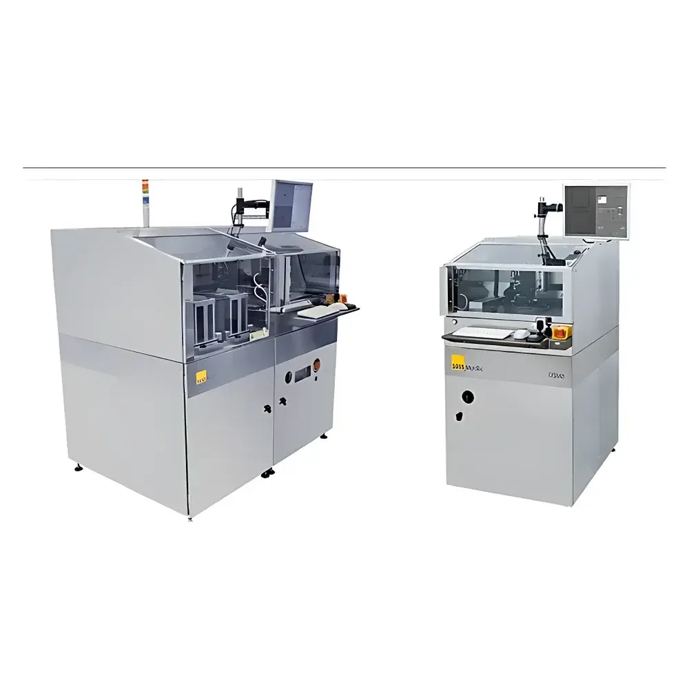
SUSS DSM8/200 Gen2 Dual-Side Alignment Metrology System
| Brand | SUSS MicroTec |
|---|---|
| Origin | Germany |
| Model | DSM8/200 Gen2 |
| Measurement Principle | Dual-microscope optical alignment metrology with TIS-compensated image registration |
| Accuracy | ≤ 0.2 µm (after TIS compensation) |
| Configuration Options | Manual loading (DSM8 Gen2) / Robotic handling with custom chuck (DSM200 Gen2) |
| Illumination Options | Visible + optional IR illumination (for through-silicon feature imaging) |
| Software Platform | Cognex PatMax®-powered automated image analysis with recipe-driven operation |
| Compliance Context | Designed for GLP/GMP-aligned semiconductor process development and high-reliability packaging workflows |
Overview
The SUSS DSM8/200 Gen2 Dual-Side Alignment Metrology System is an engineered solution for high-precision overlay verification in double-sided lithography, wafer-level packaging, and advanced MEMS, power semiconductor, and photonic device fabrication. Based on a dual-microscope optical architecture—distinct from single-microscope through-substrate imaging—the system eliminates systematic errors induced by diffraction artifacts, lens distortion, and mechanical stage wobble. It quantifies alignment offset vectors across three orthogonal degrees of freedom: translational displacement (X, Y), rotational misalignment (θ), and z-axis “wobble” (tilt-induced lateral shift). Unlike conventional alignment tools that infer backside registration indirectly, the DSM8/200 Gen2 acquires simultaneous, co-registered images of front-side and backside alignment marks using two independent, fixed-position microscopes. This rigid, non-scanning optical path ensures measurement stability over time and thermal drift, making it suitable for both R&D process qualification and high-volume production line integration.
Key Features
- Dual-microscope optical design with fixed-focus, non-moving imaging paths—eliminates stage-induced TIS (Tool Induced Shift) and improves repeatability
- TIS compensation protocol: automatic comparison of measurements at 0° and 180° substrate rotation, enabling sub-200 nm accuracy after correction
- Cognex PatMax® vision engine integrated natively—provides robust pattern recognition under variable contrast, partial occlusion, and low-SNR conditions typical in metal-layer or oxide-aligned marks
- Modular platform: DSM8 Gen2 supports manual substrate loading for lab-scale process development; DSM200 Gen2 adds robotic handler with customizable vacuum chucks and edge-grip solutions for 150 mm to 200 mm wafers and diced substrates
- Optional infrared illumination module (940 nm) enables visualization and measurement of alignment features embedded beneath silicon substrates up to 725 µm thick—critical for through-silicon via (TSV) and silicon interposer applications
- Compact footprint (< 1.2 m²) minimizes cleanroom space requirements while maintaining full alignment metrology capability
Sample Compatibility & Compliance
The DSM8/200 Gen2 accommodates a broad range of substrate types and configurations: bare silicon, SOI, glass, sapphire, GaAs, and compound semiconductor wafers from 100 mm to 200 mm diameter; diced die on carrier frames; and heterogeneous stacked assemblies with polymer or metal redistribution layers. Its measurement methodology complies with fundamental principles outlined in SEMI E10 (Specification for Definition and Measurement of Equipment Reliability, Maintainability, and Availability) and aligns with traceability frameworks required for ISO 9001-certified process development labs. While not a production lithography tool, its metrology output serves as objective evidence for process capability studies referenced in IATF 16949 and AEC-Q200 qualification workflows. Data integrity is maintained via audit-trail-enabled software logging, supporting internal GLP documentation and FDA 21 CFR Part 11 readiness when deployed in regulated packaging environments.
Software & Data Management
Operation is governed by a recipe-driven user interface with configurable measurement sequences, exposure presets, and pass/fail thresholds per alignment layer. All measurement data—including raw images, registered coordinates, residual error vectors, and TIS correction logs—are timestamped and stored in structured CSV and HDF5 formats. The system supports direct export to industry-standard SPC platforms (e.g., InfinityQS, Minitab) and integrates with factory MES via OPC UA or SECS/GEM protocols. Image archives are indexed by lot ID, wafer map position, and operator ID, ensuring full traceability. PatMax® calibration routines are executed automatically during startup and after environmental perturbations (e.g., ambient temperature shift > 1.5°C), preserving long-term measurement fidelity without manual intervention.
Applications
- Double-sided lithography validation for MEMS inertial sensors and pressure transducers requiring front-to-back critical dimension alignment
- Wafer-level chip-scale packaging (WLCSP) where redistribution layer (RDL) alignment to underlying die pads must be verified pre-bumping
- Power device manufacturing involving SiC or GaN die attach on ceramic or metal-core substrates with fiducial-based placement verification
- Photonic integrated circuit (PIC) assembly, including edge-coupled laser diode alignment to silicon nitride waveguides
- Process window characterization for stepper/scanner overlay control in pilot-line development
- Failure analysis root cause determination when electrical test yields correlate with observed alignment drift
FAQ
What substrate thicknesses support IR-based backside imaging?
IR illumination enables reliable feature detection through silicon substrates up to 725 µm thick; performance degrades gradually beyond this limit depending on doping concentration and surface roughness.
Is the system compatible with non-circular substrates or irregularly shaped dies?
Yes—custom chuck designs and PatMax®’s geometric model training allow measurement on rectangular, square, or freeform substrates when fiducials are present and optically resolvable.
How frequently is recalibration required?
System-level calibration (microscope pixel mapping, illumination uniformity, and TIS baseline) is performed semi-annually or after major maintenance; daily verification uses built-in reference targets with NIST-traceable dimensional certification.
Can the DSM200 Gen2 integrate into an existing cluster tool environment?
Yes—robotic interface conforms to SEMI E47.1 standards; load port height, FOUP/FOSB compatibility, and SECS/GEM messaging are configurable per fab integration requirements.
Does the system support real-time feedback to lithography tools?
While not a closed-loop controller, measurement reports can trigger automated alerts or feed forward offsets to compatible steppers via standardized data exchange protocols (e.g., GEM300-compliant overlay correction files).


