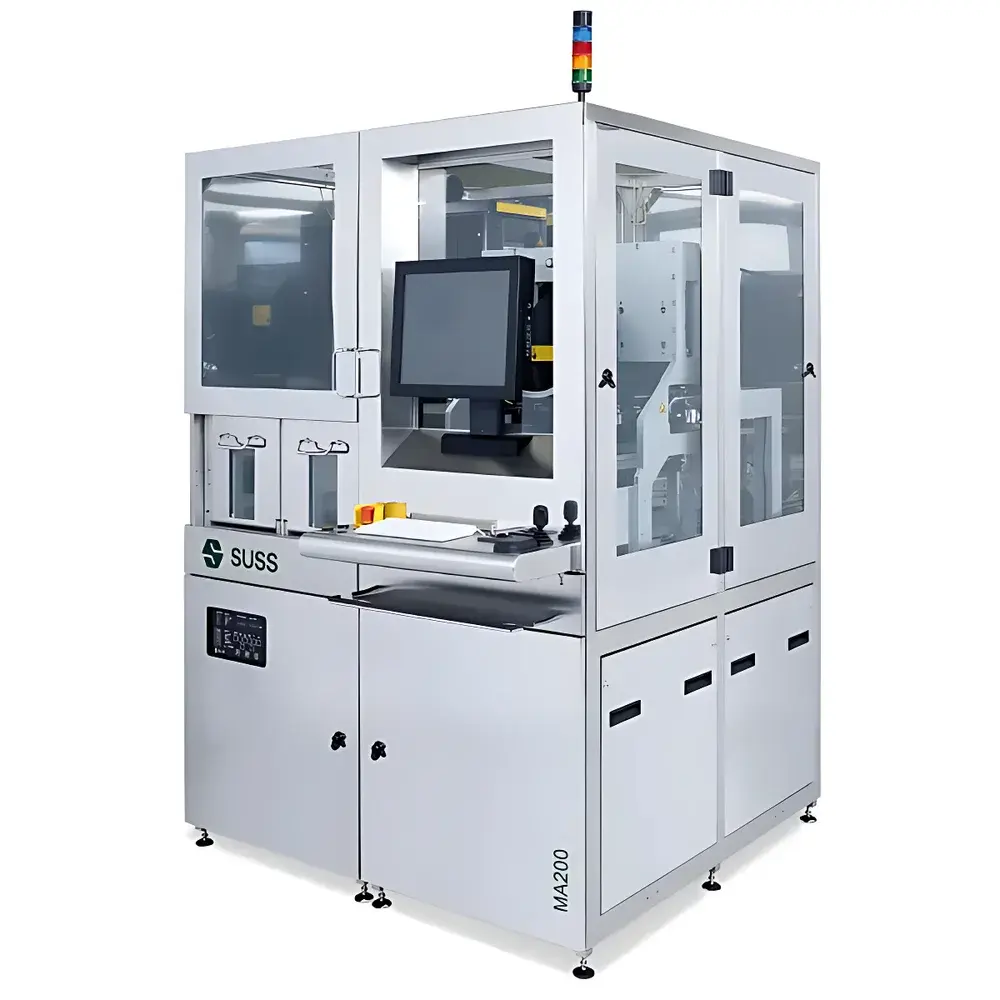
SUSS MA200 Gen3 Mask Aligner
| Brand | SUSS MicroTec |
|---|---|
| Origin | Germany |
| Manufacturer Type | Authorized Distributor |
| Origin Category | Imported |
| Model | SUSS MA200 Gen3 |
| Pricing | Upon Request |
Overview
The SUSS MA200 Gen3 Mask Aligner is a fully automated, high-throughput photolithography system engineered for precision mask-to-wafer alignment and exposure of substrates up to 200 mm in diameter—including square reticles and MEMS wafers. Based on contact/near-contact lithography principles, the MA200 Gen3 delivers sub-micron resolution through controlled proximity, soft/hard contact, and vacuum contact exposure modes. Its core architecture integrates real-time vision-based alignment (DirectAlign® with PatMax®), thermally stabilized MO® illumination optics, and modular handling platforms—making it a production-grade solution for advanced packaging, MEMS, RF devices, power semiconductors, image sensors, and compound semiconductor fabrication where overlay accuracy, process stability, and yield consistency are mission-critical.
Key Features
- DirectAlign® with PatMax® real-time pattern recognition: Achieves ≤0.5 µm top-side alignment accuracy without reliance on stored reference images—ensuring robust registration across wafer batches and thermal drift conditions.
- MO® (Modular Optics) illumination system: Delivers uniform irradiance (±2% across 200 mm field) and long-term intensity stability (<0.5% drift over 8 h); supports rapid switching between High-Resolution (HR) and Low-Glare Optical (LGO) modes via plug-and-play optical modules.
- Far-field telecentric illumination: Expands depth-of-focus and process window for thick resists and warped substrates; compatible with optional reduction kits for <150 mm wafers and custom bandpass filters (e.g., i-line, g-line, broadband UV).
- Multi-mode exposure capability: Supports proximity mode (≥3.5 µm resolution), soft/hard contact mode (≤1.0 µm), and vacuum contact mode (≤0.8 µm)—all configurable within a single platform without hardware reconfiguration.
- Advanced substrate handling: Dual-stage chuck with independent vacuum zoning accommodates fragile, ultra-thin (down to 50 µm), or highly warped wafers; edge-handling carriers preserve double-sided device structures during alignment and exposure.
Sample Compatibility & Compliance
The MA200 Gen3 processes standard silicon, glass, quartz, SOI, GaAs, SiC, and flexible polymer substrates ranging from 50 × 50 mm² to 200 mm diameter. It complies with SEMI S2/S8 safety standards and supports integration into Class 100 cleanroom environments. Process recipes and alignment logs are timestamped and user-auditable—enabling traceability required under ISO 9001, IATF 16949, and internal GLP/GMP workflows. While not FDA-certified as a medical device, its data integrity features—including operator login tracking, recipe versioning, and non-editable exposure logs—align with foundational expectations of 21 CFR Part 11-compliant documentation practices in regulated R&D and pilot-line manufacturing.
Software & Data Management
Controlled via SUSS’ proprietary AlignMaster® software suite, the MA200 Gen3 provides intuitive recipe-driven operation with full parameter logging (exposure dose, alignment offsets, chuck temperature, vacuum levels). All alignment events are captured as annotated image sequences with metadata export (CSV, XML) for offline metrology correlation. The system supports OPC UA connectivity for factory-level MES/SCADA integration and includes built-in diagnostics for optical throughput monitoring, lamp aging compensation, and alignment repeatability trending—facilitating predictive maintenance and SPC-based process control.
Applications
- MEMS fabrication: High-fidelity patterning of inertial sensors, pressure transducers, and microfluidic channels requiring strict overlay control across multi-layer stacks.
- Advanced packaging: Fan-out wafer-level packaging (FOWLP), redistribution layer (RDL) formation, bump lithography (Cu, Ni, SnAg), and TSV passivation.
- Image sensor manufacturing: Microlens array definition, color filter patterning, and backside illumination (BSI) processing on thinned wafers.
- Compound semiconductor devices: GaN HEMT gate patterning, SiC power diode mesa etch masks, and RF MMIC photomasks.
- Research & development: Rapid prototyping of novel optoelectronic, plasmonic, and metamaterial structures on non-standard substrates.
FAQ
What substrate sizes does the MA200 Gen3 support?
Standard configuration handles wafers from 100 mm to 200 mm diameter and square substrates up to 200 × 200 mm²; optional reduction kits enable processing of smaller formats including 76 mm, 100 mm, and 150 mm wafers.
Does the system support double-sided alignment?
Yes—the MA200 Gen3 can be equipped with an optional backside alignment module (BSA) for through-wafer registration using infrared illumination and dedicated IR-transparent alignment marks.
Is remote diagnostics and service supported?
All Gen3 systems include embedded Ethernet connectivity and SUSS Remote Service Interface (RSI), enabling secure technician-assisted troubleshooting, firmware updates, and calibration verification without on-site intervention.
Can exposure dose be precisely controlled and repeated?
Yes—integrated radiometric dosimetry (calibrated UV sensor) enables closed-loop dose control with ±1% repeatability; exposure time and intensity are independently adjustable per recipe step.
What maintenance intervals are recommended for the MO® illumination system?
Lamp replacement is recommended every 1,500–2,000 hours of operation; optical alignment verification and intensity uniformity mapping are advised quarterly or after any mechanical shock event.
Related Products


