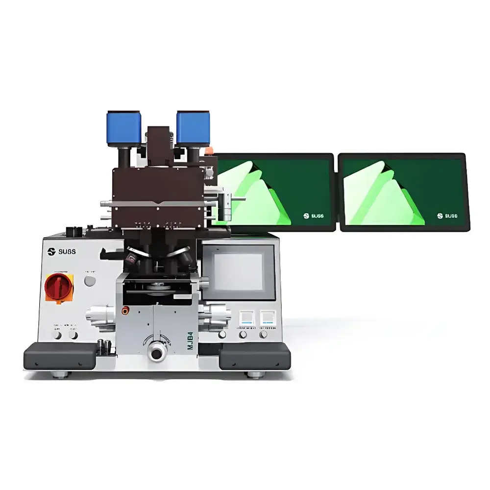
SUSS MJB4 Manual Mask Aligner
| Brand | SUSS |
|---|---|
| Origin | Germany |
| Model | MJB4 |
| Substrate Size | Up to 100 mm |
| Alignment Accuracy | Sub-micron |
| Resolution | ≤ 0.5 µm (hard contact) to 2 µm (soft contact) |
| Exposure Modes | Soft Contact, Hard Contact, Vacuum Contact |
| Optical System | MO® Exposure Optics with Telecentric Illumination |
| Uniformity | >95% across field |
| Compatible Substrates | Fragile, III-V, Compound Semiconductors, Glass, Si, SOI, Flexible Foils (thickness up to 4 mm) |
Overview
The SUSS MJB4 Manual Mask Aligner is a precision-engineered photolithography tool designed for academic research laboratories and low-volume semiconductor prototyping environments. Built upon SUSS MicroTec’s decades of expertise in contact lithography, the MJB4 implements a robust mechanical alignment architecture combined with telecentric MO® (Micro-Optics) exposure optics to deliver reproducible sub-micron pattern transfer on substrates up to 100 mm in diameter. Unlike projection steppers or scanners, the MJB4 operates on the principle of proximity or contact lithography—where a photomask is brought into controlled physical proximity or direct contact with a photoresist-coated substrate under uniform UV illumination (typically i-line at 365 nm). This approach enables high-resolution patterning without the complexity and cost of deep-UV optical reduction systems, making it particularly suitable for rapid process development, MEMS fabrication, optoelectronic device prototyping, and hybrid material integration where mask-based fidelity and process transparency are critical.
Key Features
- Sub-micron alignment accuracy enabled by high-stiffness manual X-Y-θ alignment stage with micrometer-driven fine adjustment and integrated vernier scales
- MO® exposure optics featuring micro-lens array-based homogenization for >95% irradiance uniformity across the full exposure field, extending process window and improving yield consistency
- Telecentric illumination architecture decouples lamp aging effects from exposure dose stability—ensuring consistent critical dimension (CD) control over extended lamp lifetime
- Three configurable exposure modes: soft contact (for fragile or warped substrates), hard contact (for highest resolution ≤0.5 µm), and vacuum contact (for enhanced mask-to-wafer adhesion and reduced diffraction effects)
- Modular microscope system supporting both single-field and step-and-repeat field inspection; optional IR alignment capability for opaque or multi-layer substrates
- UV-NIL (Ultraviolet Nanoimprint Lithography) upgrade path available, enabling resist-free patterning via thermal or UV-curable imprint stamps
Sample Compatibility & Compliance
The MJB4 accommodates a broad range of substrate geometries and materials—including brittle III-V wafers (e.g., GaAs, InP), thin-film SOI, glass, quartz, flexible polymer foils, and ceramic substrates—with thicknesses from 0.1 mm to 4 mm. Its open-stage design supports custom fixtures for non-standard shapes (e.g., squares, rectangles, irregular dies) down to 5 × 5 mm. The system complies with CE safety directives and meets IEC 61000-6-3/6-4 electromagnetic compatibility standards. While not certified for GMP production environments, its mechanical repeatability and traceable manual operation support GLP-aligned documentation protocols. Process parameters—including exposure time, gap distance, and alignment offset—are manually recorded and can be integrated into laboratory information management systems (LIMS) for audit-ready workflow tracking.
Software & Data Management
As a manual aligner, the MJB4 does not incorporate embedded digital control software or automated recipe storage. All operational parameters are set and verified using calibrated mechanical dials, analog timers, and optical alignment eyepieces. However, its modular architecture allows integration with external UV intensity monitors (e.g., OAI 300 series radiometers) and digital microscope cameras (e.g., Keyence VHX series) for quantitative image capture and offline metrology correlation. Users may document alignment steps and exposure logs in accordance with ISO/IEC 17025 or ASTM E2858–19 guidelines for lithographic process validation. Optional RS-232 or USB interfaces support connection to host PCs for timestamped exposure logging when paired with third-party timer modules.
Applications
- R&D-scale fabrication of MEMS sensors, RF filters, and microfluidic devices requiring high-aspect-ratio structures
- Prototyping of photonic integrated circuits (PICs) on silicon-on-insulator (SOI) and lithium niobate platforms
- Development of hybrid organic-inorganic optoelectronic devices, including perovskite solar cells and OLED backplanes
- Process qualification for UV-NIL stamp fabrication and replication studies
- Teaching and training in cleanroom-based microfabrication courses at universities and technical institutes
- Low-volume production of specialty semiconductor components where mask-based flexibility outweighs throughput requirements
FAQ
What is the maximum substrate size supported by the MJB4?
The MJB4 accepts substrates up to 100 mm in diameter or equivalent square dimensions (e.g., 100 × 100 mm), with thickness ranging from 0.1 mm to 4 mm.
Does the MJB4 support infrared (IR) alignment for opaque substrates?
Yes—optional IR alignment capability is available, enabling top-side or bottom-side alignment through silicon or other IR-transmissive carrier substrates.
Can the MJB4 be upgraded for UV-NIL processing?
Yes—the system supports factory-installed UV-NIL modules, including vacuum-assisted stamp alignment stages and UV-LED exposure heads compatible with thermoset and photocurable resists.
Is the MJB4 compliant with FDA 21 CFR Part 11 or similar regulatory frameworks?
No—the MJB4 is a manual instrument without electronic audit trails, electronic signatures, or secured user access controls required for Part 11 compliance. It is intended for R&D and non-GMP environments.
What UV wavelength is used for standard exposure?
The default mercury-vapor lamp emits broadband UV, with primary output at 365 nm (i-line); optional narrowband filters can isolate g-line (436 nm) or h-line (405 nm) as needed for specific resist sensitivities.


