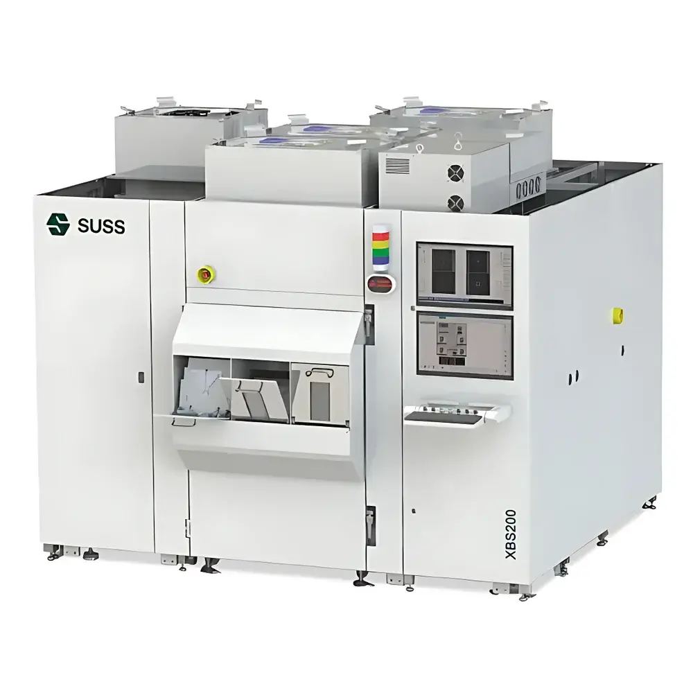
SUSS XBS200 Wafer Bonding System
| Brand | SUSS MicroTec |
|---|---|
| Origin | Germany |
| Model | XBS200 |
| Maximum Wafer Size | 200 mm |
| Bonding Force Range | 5–100 kN |
| Temperature Range | 30–500 °C |
| Heating Rate | up to 30 K/min |
| Thermal Uniformity | ±1.5 % |
| Alignment Accuracy (ISA) | < 100 nm |
| Bonding Type | Permanent (Anodic, Fusion, Glass Frit, Metal Diffusion, Eutectic, etc.) |
Overview
The SUSS XBS200 Wafer Bonding System is a high-precision, production-grade bonding platform engineered for permanent wafer-level bonding in MEMS, advanced 3D packaging, and compound semiconductor manufacturing. Based on a robust vacuum-compatible chamber architecture and precision-controlled thermal-mechanical actuation, the XBS200 implements contact-based bonding under precisely regulated force, temperature, and vacuum conditions—enabling repeatable formation of hermetic, low-defect interfaces across silicon, glass, quartz, SOI, and compound substrates (e.g., GaAs, SiC, InP). Its design adheres to semiconductor front-end and back-end process requirements, supporting both ambient and controlled-atmosphere (N₂, forming gas) bonding environments. The system is qualified for integration into ISO 9001-certified cleanroom fabs and meets mechanical safety standards per EN 60204-1 and CE machinery directives.
Key Features
- Modular, field-upgradable platform architecture supporting future expansion to additional bonding modules (e.g., plasma activation, IR pre-heating, or in-situ stress monitoring)
- Clamp-free, robotic wafer handling with non-contact edge-grip transport—eliminating mechanical distortion, particle generation, and wafer edge chipping
- Dual-zone ceramic heater with independent closed-loop PID control, enabling precise thermal profiling across the entire 200 mm wafer surface
- Sub-100 nm alignment accuracy via SUSS’ proprietary Inter-Substrate Alignment (ISA) technology integrated in the XBA Bond Aligner—achieving wafer-to-wafer (W2W) registration without reliance on global fiducials alone
- Digitally monitored bonding parameters: real-time force feedback (load cell resolution ≤ 0.1 kN), chamber pressure (10⁻⁶ mbar base vacuum), and thermal gradient mapping (≥ 32-point sensor array)
- Programmable bonding force profile (ramp-hold-relax) with active load compensation to maintain constant pressure during thermal expansion mismatch
Sample Compatibility & Compliance
The XBS200 accommodates standard 100–200 mm wafers (including thinned, warped, or patterned substrates up to 1.5 mm thickness) and supports all major permanent bonding processes: anodic, fusion, glass frit, eutectic (Au–Si, Cu–Sn), and metal diffusion bonding. It is compatible with temporary carrier bonding/debonding workflows used in thin-wafer handling. Process recipes are compliant with SEMI S2/S8 safety guidelines and support traceability per ISO 13485 (for medical device packaging) and JEDEC JEP172 (for reliability qualification of 3D ICs). Optional audit trail logging satisfies FDA 21 CFR Part 11 requirements for electronic records and signatures when paired with SUSS ProcessSuite software.
Software & Data Management
Controlled by SUSS ProcessSuite—a Windows-based, recipe-driven interface—the XBS200 provides full parameter logging (force, temperature, vacuum, time, alignment error vectors) at ≥ 10 Hz sampling rate. All data is stored in standardized SQLite databases with optional export to CSV, HDF5, or SECS/GEM-compliant formats for MES integration. The software includes built-in statistical process control (SPC) tools (X̄/R charts, Cpk calculation), automated calibration verification logs, and version-controlled recipe management with user-role access levels (Operator, Engineer, Admin). Remote diagnostics and firmware updates are supported via TLS-secured HTTPS connections, with optional OPC UA server integration for Industry 4.0 factory connectivity.
Applications
- MEMS encapsulation (e.g., gyroscopes, pressure sensors) requiring hermetic cavity sealing with minimal residual stress
- 3D heterogeneous integration: TSV-enabled stacked die bonding, interposer-to-die fusion bonding, and hybrid bonding R&D
- Micro-LED transfer and mass bonding onto display backplanes using thermal compression or metal thermo-compression
- SOI wafer reclamation via smart-cut bonding and layer splitting
- Optoelectronic packaging: InP-on-silicon photonic integration and laser diode submount bonding
- Quantum device fabrication: superconducting qubit chip bonding with ultra-low particulate and thermal budget constraints
FAQ
What wafer materials and thicknesses does the XBS200 support?
Standard silicon, fused silica, quartz, glass (Borofloat, Pyrex), SOI, and compound semiconductors (GaAs, SiC, InP) from 100–200 mm diameter and 200 µm–1.5 mm thickness.
Is the XBS200 suitable for low-temperature bonding processes?
Yes—it supports bonding down to 30 °C with high stability; optional cryo-cooling stage enables sub-ambient bonding for thermally sensitive layers.
How is alignment verified before bonding?
Through real-time ISA image correlation, followed by automated post-alignment metrology using integrated optical interferometry; results are logged and traceable per lot.
Can the system be integrated into an automated fab line?
Yes—equipped with SECS/GEM interface, FOUP/SMIF load ports (optional), and compatibility with major AMHS protocols (OHT, AGV handshaking).
Does SUSS provide process development support?
Yes—SUSS Application Labs offer joint process qualification, DOE-based recipe optimization, and failure mode analysis (FMEA) support under NDA.


