TEO OLED/QLED Device Lifetime Testing System
| Brand | TEO |
|---|---|
| Origin | Beijing, China |
| Manufacturer Type | Authorized Distributor |
| Product Origin | Domestic (China) |
| Model | OLED/QLED Device Lifetime Testing System |
| Price Range | USD 14,000 – 28,000 |
| Channel Capacity | 32 / 64 / 128 (scalable to 512 channels) |
| Operating Modes | Constant Current, Constant Voltage, Constant Luminance (user-selectable) |
| Current Output Range | 0.03 µA – 100 mA (accuracy ±1% of reading) |
| Voltage Output Range | 1.0 – 20 V (accuracy <±1%) |
| Device Architecture Support | Bottom-emission, top-emission, inverted, and standard stack configurations (customizable per device architecture) |
| Substrate Compatibility | Standard 5 cm × 5 cm |
| Temperature Range | RT+10°C to 100°C (standard) |
| Environmental Options | Inert atmosphere testing (N₂/Ar), glovebox-integrated operation, UPS-backed power supply |
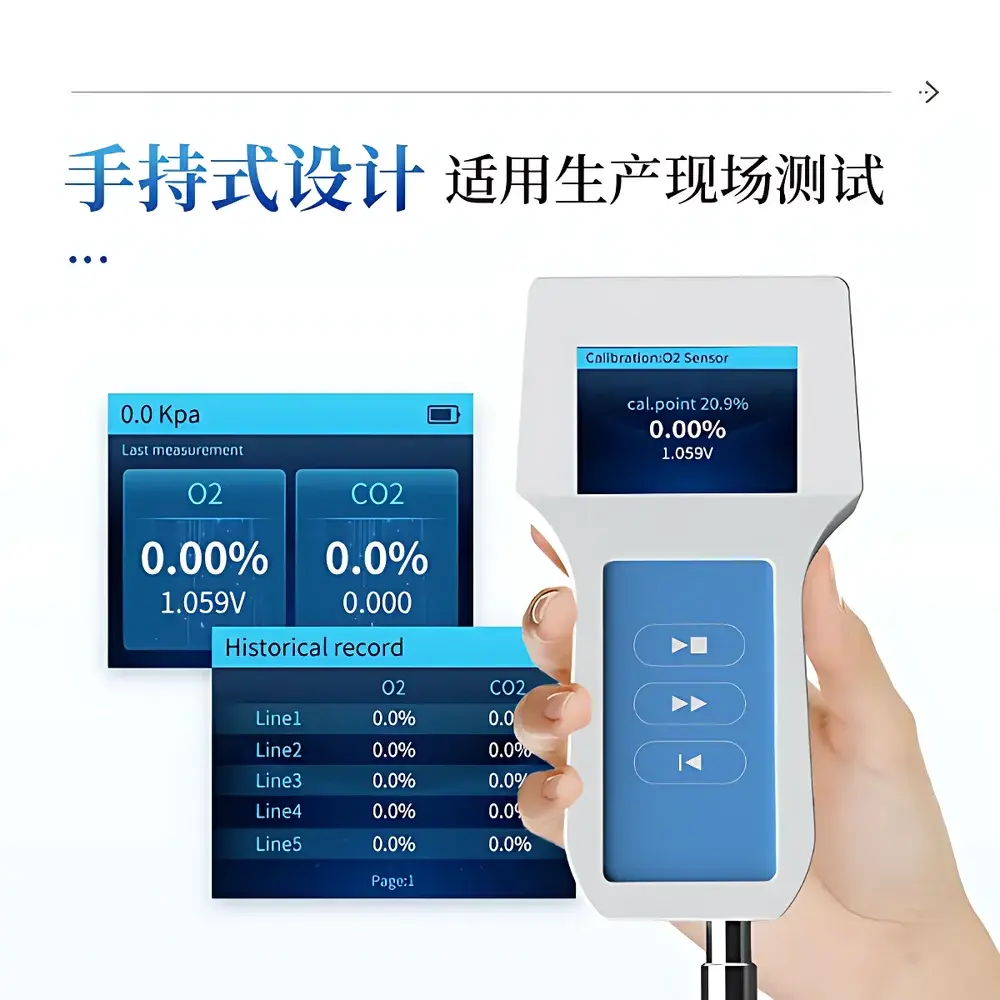
| Software Platform | LabVIEW-based control and data acquisition with real-time logging, timestamped event tracking, and export-ready CSV/Excel output |
Overview
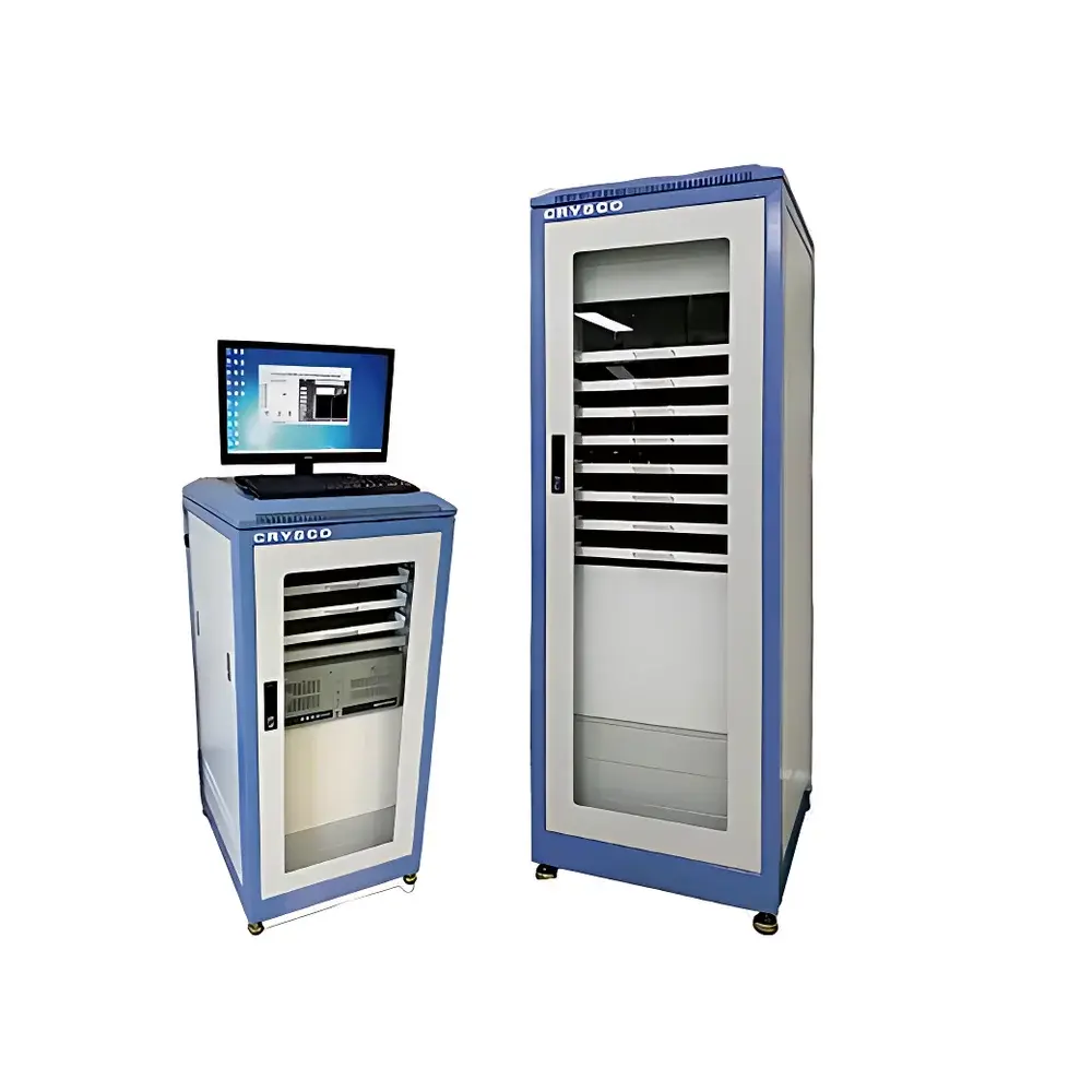
The TEO OLED/QLED Device Lifetime Testing System is a purpose-built, multi-channel accelerated aging platform engineered for quantitative operational stability assessment of organic and quantum-dot light-emitting diodes under controlled electrical, thermal, and environmental conditions. It operates on the principle of continuous or pulsed bias-driven stress testing, where luminance decay (Lₜ/L₀), voltage rise (Vₜ/V₀), and color shift (CIE Δx, Δy) are monitored in real time using integrated photometric and electrical feedback loops. Designed for R&D laboratories, display material developers, and QC facilities, the system enables compliance-aligned lifetime projection (e.g., T₅₀, T₇₀, T₉₀) in accordance with industry-standard protocols such as ISO 11664-5 (colorimetry), CIE Publication 127 (LED measurement), and JEDEC JESD22-A114 (high-temperature operating life). Its modular architecture supports scalable channel expansion—up to 512 parallel test positions—making it suitable for high-throughput screening of emissive layer formulations, encapsulation efficacy, and pixel-level degradation kinetics.
Key Features
- Multi-channel precision current/voltage sourcing with independent per-channel calibration traceability to NIST-traceable standards
- Configurable stress modes: constant-current (CC), constant-voltage (CV), constant-luminance (CL) with closed-loop photodiode feedback, and programmable pulse profiles (pulse width, duty cycle, amplitude)
- Thermally stabilized test environment with PID-controlled heating stages (RT+10°C to 100°C); optional cryogenic extension (-50°C to 100°C) for low-temperature degradation studies
- Modular fixture design accommodating bottom-emission, top-emission, inverted, and tandem OLED/QLED architectures; custom substrate holders support up to 20 cm × 20 cm active areas
- Integrated ambient control options: inert gas purging (N₂/Ar), glovebox integration (O₂/H₂O < 0.1 ppm), and uninterruptible power supply (UPS) for continuity-critical long-term tests (>1,000 hrs)
- LabVIEW-based software with audit-trail-enabled data acquisition, automated pass/fail thresholding, and GLP-compliant metadata tagging (operator ID, test start/end timestamps, environmental logs)
Sample Compatibility & Compliance
The system accommodates a broad spectrum of emissive device formats—including small-molecule OLEDs, polymer LEDs (PLEDs), QLEDs, PeLEDs, and micro-LED hybrids—across varying substrate types (glass, flexible PET/PI, silicon wafers). Electrical interface is compatible with standard probe stations and ZIF sockets. All hardware and software modules comply with CE marking requirements and meet electromagnetic compatibility (EMC) Class B limits per EN 61326-1. Data integrity features—including electronic signatures, version-controlled script deployment, and immutable raw-data archives—support alignment with FDA 21 CFR Part 11 and ISO/IEC 17025 documentation requirements for accredited testing labs.
Software & Data Management
The embedded LabVIEW application provides synchronized acquisition of luminance (via calibrated Si photodiodes), forward voltage, current, and thermocouple readings at user-defined intervals (100 ms to 1 hr resolution). Each channel maintains an independent dataset with automatic interpolation for missing points due to transient sensor dropout. Export formats include UTF-8 CSV, Excel (.xlsx), and HDF5 for downstream statistical modeling (e.g., Weibull analysis, Arrhenius extrapolation). Audit logs record all parameter changes, manual interventions, and calibration events with SHA-256 hashing for tamper detection. Remote monitoring is supported via secure HTTPS API endpoints, enabling integration into enterprise LIMS environments.
Applications
- Accelerated lifetime validation of novel host/emitter materials under constant or pulsed drive conditions
- Encapsulation barrier performance evaluation under thermal-humidity stress (85°C/85% RH) and oxygen exposure
- Pixel-level uniformity mapping and failure mode analysis (dark spot growth, edge delamination, cathode oxidation)
- Comparative reliability benchmarking across fabrication batches, deposition methods (evaporation vs. inkjet), and TFT backplane integrations
- Support for JEDEC JESD22-A108 (temperature cycling) and IEC 61238-1 (humidity testing) derivative test plans
FAQ
What is the maximum number of devices that can be tested simultaneously?
Up to 512 devices may be monitored concurrently through modular channel expansion; base configurations support 32, 64, or 128 channels.
Can the system operate inside a nitrogen-filled glovebox?
Yes—custom feedthroughs, sealed cable glands, and low-outgassing components enable seamless integration into Class 1000 or better inert-atmosphere gloveboxes.
Is photometric calibration included with the system?
Each unit ships with factory-calibrated photodiodes traceable to NIST SRM 2241; optional annual recalibration services are available.
Does the software support automated reporting for regulatory submissions?
Yes—the LabVIEW platform generates PDF reports with embedded metadata, statistical summaries, and raw-data appendices compliant with ISO 17025 technical records requirements.
What is the typical lead time for custom fixture development?
Standard 5 cm × 5 cm fixtures ship with the system; custom substrates up to 20 cm × 20 cm require 4–6 weeks from mechanical drawing approval.