Thicktest SKT-500 Fourier Transform Infrared (FTIR) Spectrometer with Reflectance Mode and Integrated Infrared Microscopy for Epitaxial Layer Thickness Metrology
| Brand | Thicktest |
|---|---|
| Origin | Shaanxi, China |
| Manufacturer Type | Direct Manufacturer |
| Country of Origin | Domestic (China) |
| Model | SKT-500 |
| Pricing | Upon Request |
Overview
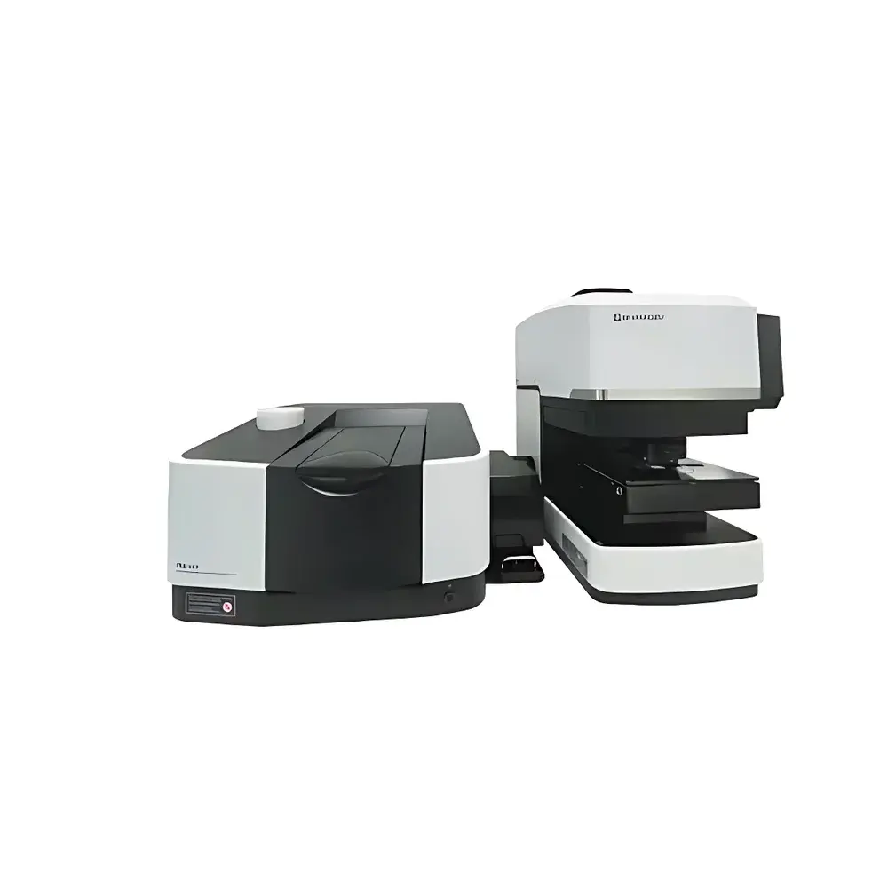
The Thicktest SKT-500 is a benchtop Fourier Transform Infrared (FTIR) spectrometer engineered for high-precision, non-destructive thickness metrology of semiconductor epitaxial layers—particularly silicon carbide (SiC), gallium nitride (GaN), and other wide-bandgap compound semiconductors. It operates in reflectance mode across the mid-infrared spectral range (typically 4000–400 cm⁻¹, corresponding to 2.5–25 µm wavelength), where optical interference fringes generated at layer interfaces are highly sensitive to film thickness in the micrometer scale. Unlike UV-Vis reflectance or Fabry–Pérot-based methods that rely on empirical approximations and fixed refractive index assumptions, the SKT-500 implements a physically self-consistent dielectric modeling framework. This approach fits the entire measured reflectance spectrum—rather than isolated fringe peaks—against a multi-layer optical transfer matrix model, enabling robust extraction of thickness without prior knowledge of complex refractive index dispersion or damping parameters. The system integrates an infrared microscope for spatially resolved mapping, supporting wafer-level characterization with spot sizes down to 15 µm (dependent on objective lens and aperture configuration).
Key Features
- Mid-infrared FTIR platform with KBr beam splitter and DTGS detector (optional MCT for enhanced SNR)
- Dedicated reflectance measurement geometry optimized for semiconductor wafers (4″–6″ diameter compatible)
- Integrated infrared microscope with motorized XYZ stage and selectable objectives (e.g., 15×, 32× reflective objectives)
- Full-spectrum physical modeling engine based on Fresnel equations and transfer-matrix formalism
- No requirement for pre-assigned refractive index values: simultaneous fitting of thickness, background carrier concentration (via free-carrier absorption modeling), and interfacial roughness
- Support for single-layer and multi-layer epitaxial stack analysis—including graded or compositionally varying layers
- Compliant with ISO/IEC 17025 traceability principles for calibration; supports NIST-traceable reference standards
Sample Compatibility & Compliance
The SKT-500 accommodates polished, uncoated SiC, GaN, Si, and AlN wafers ranging from 50 mm to 150 mm in diameter. It requires no vacuum or cryogenic environment and functions under ambient laboratory conditions. Measurements are insensitive to surface oxidation or native oxide layers ≤2 nm, provided the oxide is stoichiometric and uniform. For regulatory environments, data acquisition and processing workflows support audit trails compliant with FDA 21 CFR Part 11 when deployed with Thicktest’s optional secure software package (version 3.2+). All spectral data files adhere to JCAMP-DX v6.00 format, ensuring interoperability with third-party analysis tools used in GLP/GMP-compliant labs. The instrument meets IEC 61000-6-3 (EMC emission) and IEC 61010-1 (safety) standards for laboratory equipment.
Software & Data Management
Control and analysis are executed via Thicktest IRPro Suite—a Windows-based application built on Qt and Python 3.9 backend. Core modules include real-time interferogram monitoring, automated baseline correction using asymmetric least squares (AsLS), and nonlinear least-squares fitting using Levenberg–Marquardt optimization. The software stores all raw interferograms, processed spectra, fit parameters, and uncertainty estimates in HDF5 containers with embedded metadata (sample ID, operator, timestamp, instrument configuration). Export options include CSV, ASCII, and industry-standard .SPA formats. Version-controlled method templates allow replication across shifts and facilities; user roles (Operator, Analyst, Administrator) enforce access control per ISO 17025 Section 6.2 requirements.
Applications
- Quantitative thickness mapping of SiC homoepitaxial layers (1–200 µm range) for power device fabrication
- Multi-layer stack characterization in GaN-on-Si or AlGaN/GaN heterostructures
- Correlation of free-carrier concentration profiles with reflectance phase shift in doped epilayers
- Process validation and SPC tracking during MOCVD or CVD epitaxy runs
- Failure analysis of delamination or interfacial void formation via spectral residual analysis
- Research-grade optical constant determination for novel wide-bandgap materials (e.g., β-Ga₂O₃, diamond)
FAQ
What spectral range does the SKT-500 cover, and why is mid-IR optimal for SiC epitaxial thickness?
The system operates from 4000 to 400 cm⁻¹ (2.5–25 µm), matching the characteristic absorption and interference scales of micrometer-thick SiC layers. Longer wavelengths yield higher fringe density per unit thickness, improving resolution beyond UV-Vis limitations.
Can it distinguish between doping-induced and thickness-induced spectral changes?
Yes—by jointly fitting thickness, carrier concentration (via Drude model), and surface/interface parameters, the algorithm decouples electronic and geometric contributions to the reflectance response.
Is cross-sectional SEM still required for validation?
While SEM remains a reference technique, the SKT-500 achieves sub-1% relative thickness uncertainty on certified SiC standards, making it suitable as a primary metrology tool in production environments where throughput and non-destructiveness are critical.
Does the system support automated wafer scanning?
Yes—motorized X-Y stages with programmable grid patterns enable full-wafer thickness uniformity mapping (e.g., 9-point or 25-point radial scans) with configurable dwell time and spectral averaging.
How is calibration maintained over time?
A dual-reference protocol is implemented: daily verification using a NIST-traceable polystyrene film standard, and quarterly full-system alignment using He–Ne laser interferometry and blackbody source characterization.


