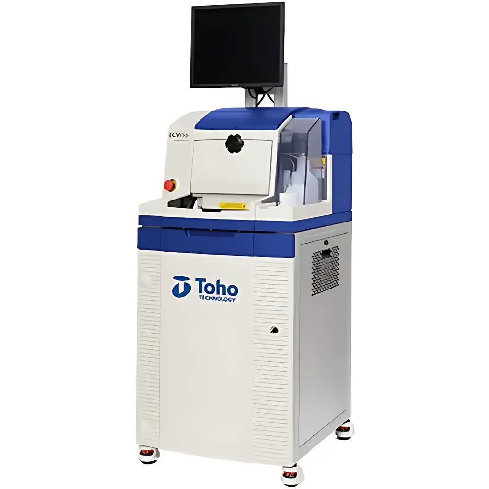
Toho ECVpro+ Electrochemical Capacitance-Voltage Profiler
| Brand | Toho |
|---|---|
| Origin | Japan |
| Model | ECVpro+ |
| Measurement Principle | Electrochemical C–V Profiling |
| Carrier Concentration Range | 1×10¹¹ to 1×10²¹ cm⁻³ |
| Depth Resolution | Down to ≤1 nm |
| Sample Compatibility | Si, Ge, SiC, GaAs, InP, GaN, AlGaN, InGaN, AlInN, ZnO, CdTe, HgCdTe, and multicomponent III–V/II–VI semiconductors |
| Automation Level | Fully Automated (Dry-In/Dry-Out, Auto-Load/Unload/Reload) |
| System Architecture | Modular, Cleanroom-Compatible, Optically & Electrically Isolated Subsystems |
Overview
The Toho ECVpro+ Electrochemical Capacitance-Voltage Profiler is a high-precision, fully automated analytical instrument engineered for quantitative depth-resolved carrier concentration profiling in semiconductor materials. It operates on the electrochemical capacitance–voltage (ECV) principle—where a controlled anodic etching process, driven by a potentiostatic or galvanostatic bias in a tailored electrolyte, sequentially removes material layer-by-layer while continuously measuring junction capacitance as a function of applied voltage. From the resulting C–V curves, the built-in algorithm computes dopant concentration (NA/ND) versus depth with sub-nanometer vertical resolution. Unlike conventional secondary ion mass spectrometry (SIMS) or spreading resistance profiling (SRP), ECV does not require ultra-high vacuum, radioactive sources, or destructive physical sectioning—making it uniquely suited for rapid R&D iteration, epitaxial process monitoring, and failure analysis in compound semiconductor development.
Key Features
- Modular cleanroom-compatible architecture with physically isolated optical, electronic, fluidic, and electrochemical subsystems—ensuring long-term measurement stability and minimizing cross-talk interference.
- Sub-1 nm depth resolution enabled by real-time etch rate monitoring via integrated color CCD imaging and synchronized capacitance acquisition at up to 100 Hz sampling rate.
- Self-calibrating electronics: zero user-performed hardware calibration required; automatic compensation for cable capacitance, electrode polarization drift, and electrolyte conductivity variation.
- Dry-In/Dry-Out automation: robotic sample handling supports wafer-level (up to 200 mm) and chip-level (4 × 2 mm minimum) measurements with programmable Auto-Load/Unload/Reload sequences.
- Intuitive Windows-based control software with preconfigured measurement templates, user-defined experiment trees, role-based access control, and full audit trail logging compliant with GLP/GMP documentation requirements.
- Multi-material compatibility: validated protocols for elemental (Si, Ge), wide-bandgap (SiC, GaN, AlGaN, InGaN), ternary and quaternary III–V (AlGaAs, GaInP, AlGaInP), II–VI (ZnO, CdTe, HgCdTe), and emerging chalcogenide semiconductors.
Sample Compatibility & Compliance
The ECVpro+ accepts planar semiconductor samples regardless of substrate conductivity—fully compatible with insulating substrates (e.g., sapphire, SiO2/Si), semi-insulating wafers (e.g., Fe-doped InP), and conductive bulk crystals. No ohmic back contact is required; measurement relies solely on the Schottky or depletion junction formed between the electrolyte and the top surface. The system supports standardized formats from diced chips (≥4 × 2 mm) to full 8-inch (200 mm) wafers. All electrolyte chemistries are selected per material class and rigorously validated against ASTM F1756–21 (Standard Guide for Electrical Characterization of Semiconductor Epitaxial Layers) and ISO/IEC 17025 traceability frameworks. Instrument firmware and software comply with FDA 21 CFR Part 11 for electronic records and signatures where deployed in regulated manufacturing environments.
Software & Data Management
Control and analysis are executed through Toho’s proprietary ECVStudio software—a modular, object-oriented application built on .NET Framework with native support for Windows 10/11 (64-bit). The interface provides live visualization of capacitance transients, real-time etch front tracking via image overlay, and dynamic adjustment of voltage sweep parameters during acquisition. Raw data (C–V, dC/dV, time-stamped images, etch rate logs) are stored in HDF5 format with embedded metadata (operator ID, timestamp, electrolyte lot, calibration epoch). Export options include CSV, MATLAB (.mat), and industry-standard VAMPIRE-compatible XML. Audit trails record all user actions—including parameter edits, recipe modifications, and data exports—with immutable timestamps and digital signature binding. Optional integration with LIMS or MES systems is supported via OPC UA and RESTful API endpoints.
Applications
The ECVpro+ serves critical functions across semiconductor R&D and pilot-line manufacturing: quantifying dopant activation efficiency in MOCVD/MBE-grown GaN HEMT heterostructures; validating dopant diffusion profiles after thermal annealing in SiC power devices; characterizing unintentional background doping in InP-based photonic integrated circuits; mapping carrier compensation in ZnO-based transparent conductors; and verifying junction depth uniformity in multi-junction solar cells (e.g., GaInP/GaAs/Ge). It is widely referenced in peer-reviewed literature for benchmarking new dopants (e.g., Mg in GaN, Sn in InP), calibrating TCAD simulations, and qualifying novel wet etchants for PEC processing. Its non-destructive, solution-phase methodology makes it indispensable for low-yield prototype evaluation where material conservation is paramount.
FAQ
What semiconductor materials are supported out-of-the-box?
The ECVpro+ includes pre-validated electrolyte recipes and voltage protocols for Si, Ge, SiC, GaAs, InP, GaN, AlGaN, InGaN, ZnO, CdTe, and HgCdTe. Custom protocols for other materials—including emerging perovskites and 2D TMDs—are developed collaboratively with Toho’s Applications Engineering team.
Is back-side metallization required?
No. ECV relies on front-side electrolytic contact only. Insulating substrates (e.g., sapphire, quartz, glass) are fully supported without any substrate modification.
How is depth resolution determined?
Depth resolution depends on etch rate stability, signal-to-noise ratio of capacitance measurement, and electrolyte selectivity—not instrument hardware alone. For optimized conditions on GaN, reproducible ≤1 nm depth increments are routinely achieved; on slower-etching materials like SiC, typical resolution ranges from 2–5 nm.
Can the system be integrated into a Class 100 cleanroom?
Yes. The ECVpro+ meets SEMI S2/S8 safety standards and features HEPA-filtered internal air circulation, sealed fluid pathways, and vibration-isolated optical bench—enabling direct installation in ISO Class 5 environments.
Does the software support 21 CFR Part 11 compliance?
Yes. With optional validation package, ECVStudio provides electronic signatures, audit trail archiving, role-based permissions, and secure data encryption aligned with FDA 21 CFR Part 11 and EU Annex 11 requirements.


