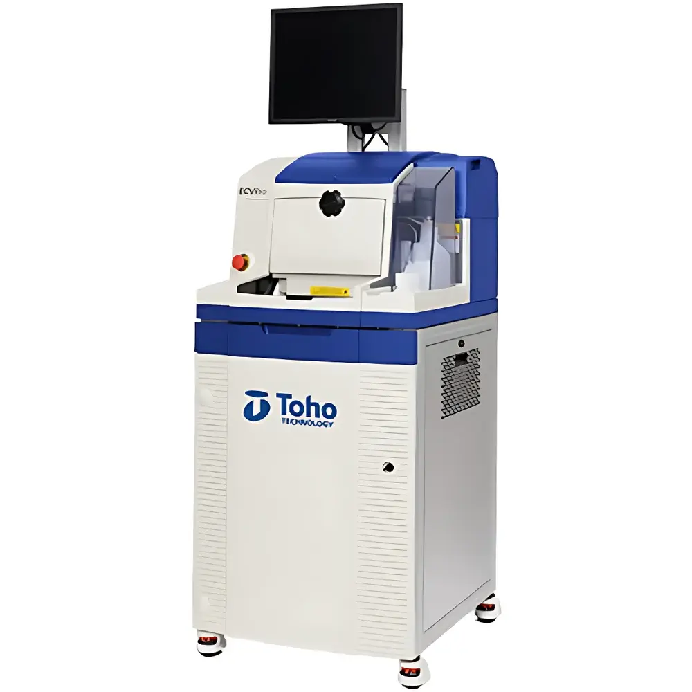
Toho ECVpro+ Electrochemical Capacitance-Voltage Profiler
| Brand | Toho |
|---|---|
| Origin | Japan |
| Model | ECVpro+ |
| Carrier Concentration Range | 1×10¹¹ to 1×10²¹ cm⁻³ |
| Depth Resolution | down to ≤1 nm |
| Sample Compatibility | Si, Ge, SiC, GaAs, InP, GaN, AlGaN, InGaN, AlInN, ZnO, CdTe, HgCdTe, and other III–V, II–VI, IV–IV, and ternary/quaternary compound semiconductors |
| Automation Level | Fully automated electrochemical etching and C–V scanning |
| Compliance | Designed for GLP/GMP-aligned R&D and process development environments |
Overview
The Toho ECVpro+ Electrochemical Capacitance-Voltage Profiler is a precision metrology instrument engineered for quantitative depth-resolved carrier concentration profiling in semiconductor epitaxial layers, bulk substrates, and heterostructures. It operates on the fundamental principle of electrochemical capacitance–voltage (ECV) analysis: a controlled anodic etch—driven by a potentiostatically regulated electrolyte—progressively removes material layer-by-layer while simultaneously measuring junction capacitance as a function of applied DC bias. From the resulting C–V curves, the carrier concentration profile ND(x) or NA(x) is derived using the standard Mott–Schottky relationship (1/C² ∝ V), enabling nanoscale vertical resolution without ion beam sputtering or destructive cross-sectioning. Developed from legacy platforms originally commercialized by Bio-Rad and Accent Optical Technologies—and refined over three decades of industrial deployment—the ECVpro+ integrates robust electrochemical cell design, low-noise high-impedance capacitance measurement circuitry, and deterministic real-time etch monitoring to deliver reproducible, traceable dopant distribution data essential for epitaxial process validation, defect engineering, and device simulation calibration.
Key Features
- Fully automated electrochemical etching and C–V acquisition sequence under software-defined voltage sweep, current limit, and etch rate control
- Modular architecture with physically isolated optical, electronic, fluidic, and mechanical subsystems—minimizing cross-talk and enabling maintenance without system recalibration
- Self-calibrating capacitance measurement electronics: eliminates manual cable compensation or reference capacitor adjustments; maintains accuracy across thermal drift and long-term operation
- Integrated color digital camera system for real-time visualization and documentation of sample surface morphology before, during, and after etching—enabling correlation of electrical profiles with physical features (e.g., interfacial roughness, pit formation, or selective etch stop)
- Dry-in/Dry-out sample handling with auto-load/unload/reload capability for wafers up to 200 mm (8-inch); compatible with diced chips (≥4 × 2 mm) and non-standard geometries via custom fixtures
- Configurable measurement menus with user-definable priority levels—supports rapid method transfer between labs and integration into standardized semiconductor characterization workflows
Sample Compatibility & Compliance
The ECVpro+ accommodates a broad spectrum of semiconductor materials without requiring substrate conductivity. It has been validated on conductive (e.g., n⁺-Si, GaN-on-Si), semi-insulating (e.g., Fe-doped InP, semi-insulating GaAs), and dielectric-buffered structures (e.g., SiO₂/Si, Al₂O₃/GaN). Material coverage includes elemental semiconductors (Si, Ge), wide-bandgap compounds (SiC, GaN, AlGaN, InGaN, AlInN), III–V binaries and alloys (GaAs, InP, AlGaAs, InGaP, AlInAs, AlGaInP), II–VI systems (ZnO, CdTe, HgCdTe), and emerging chalcogenides and oxides. Each material class requires selection of a chemically matched electrolyte (e.g., HF-based for Si, KOH/ethylene glycol for GaN, bromine-methanol for III–V arsenides)—a protocol library is embedded in the software with safety-rated fluid handling and waste neutralization modules. The system supports audit-ready operation per ISO/IEC 17025 principles and includes optional 21 CFR Part 11-compliant electronic signatures, audit trails, and role-based access control for regulated R&D and pilot-line environments.
Software & Data Management
Control and analysis are executed via Toho’s proprietary ECV-Studio software suite—a Windows-based application built on deterministic real-time threading and deterministic I/O scheduling. The interface provides synchronized display of capacitance transients, etch current, stage position, and live video feed. Raw C–V datasets are stored in HDF5 format with embedded metadata (date/time, operator ID, sample ID, electrolyte lot, calibration timestamp). Profile extraction uses iterative deconvolution algorithms that account for series resistance, interface state density, and non-ideal junction behavior—results export to CSV, MATLAB .mat, and industry-standard SDF (Semiconductor Data Format) for import into TCAD tools (e.g., Sentaurus, Silvaco Atlas). Batch processing, statistical trend reporting, and pass/fail thresholding against specification limits are supported for process qualification studies.
Applications
- Epitaxial layer verification: thickness, doping uniformity, abruptness, and background carrier concentration in MOCVD/MBE-grown GaN HEMTs, SiC power diodes, and InP-based photonics
- Ion implantation dose and depth profiling—particularly for ultra-shallow junctions (<50 nm) where SIMS sensitivity degrades
- Diffusion studies in annealed structures (e.g., B diffusion in Si, Mg activation in GaN)
- PEC (photoelectrochemical) etch mechanism analysis—including etch selectivity, surface recombination effects, and photo-carrier-assisted dissolution kinetics
- Quality assurance of commercial epiwafers prior to device fabrication—used by foundries and compound semiconductor suppliers for PQ (Process Qualification) and FA (Failure Analysis) support
FAQ
What electrolytes are supported, and how is compatibility determined?
Electrolyte selection is material-specific and based on thermodynamic stability windows and etch selectivity data. Toho provides validated protocols for >30 semiconductor systems; custom electrolyte development is available under NDA.
Does the system require periodic hardware recalibration?
No—capacitance electronics perform automatic self-calibration at startup and during idle cycles. Only routine verification using certified reference samples (e.g., calibrated Si standards) is recommended per ISO/IEC 17025 internal quality procedures.
Can the ECVpro+ measure insulating layers or buried interfaces?
Yes—provided the underlying layer is conductive or semi-conductive and forms a rectifying junction with the electrolyte. Insulating capping layers (e.g., SiO₂, AlN) can be pre-etched or patterned to expose the active region.
Is remote operation and monitoring supported?
The system supports secure remote desktop access and real-time data streaming via TLS-encrypted Ethernet; full control requires local administrator privileges per cybersecurity policy.
What level of technical support and service coverage is provided?
Toho offers global field service, application engineering support, preventive maintenance contracts, and on-site training programs aligned with SEMI E10 and E136 standards for equipment reliability and uptime management.


