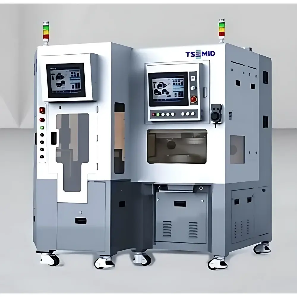
TSD IVG-2040 / IVG-3040 Fully Automated Single-Axis Wafer Thinning System
| Brand | TSD |
|---|---|
| Model | IVG-2040 / IVG-3040 |
| Max Wafer Size | 200 mm (8") / 300 mm (12") |
| Grinding Wheel OD | 203 mm / 303 mm |
| Spindle Power | 6.0 kW / 9.5 kW |
| Spindle Speed | 0–6000 rpm / 0–4000 rpm |
| Table Speed | 0–380 rpm |
| Z-Axis Feed Rate | 0.1–1000 µm/sec |
| In-Line Thickness Measurement Repeatability | ±0.001 mm |
| In-Line Thickness Range (OMM) | 0–4800 µm |
| Integrated Auto Load/Unload | Yes |
| Non-Contact Gauging (NCG) | Optional |
Overview
The TSD IVG-2040 and IVG-3040 are fully automated single-axis wafer thinning systems engineered for precision backgrinding of semiconductor wafers, optical substrates, and advanced functional materials. Based on deterministic mechanical grinding principles—utilizing high-rigidity spindle architecture, closed-loop Z-axis motion control, and real-time in-process thickness monitoring—these systems deliver sub-micron repeatability in material removal while preserving wafer flatness, surface integrity, and edge strength. Designed for integration into front-end and back-end semiconductor fabrication lines, the IVG platform supports both batch and inline processing workflows under cleanroom-compatible environmental conditions (Class 100–1000). Its core function is controlled, sequential material removal via diamond-impregnated grinding wheels, with process stability maintained through adaptive load compensation and thermal drift mitigation strategies.
Key Features
- Fully integrated auto-load/unload system with robotic wafer handling, cassette-to-cassette operation, and dry-in/dry-out workflow compliance
- High-precision in-line optical micrometer measurement (OMM) with ±0.001 mm repeatability across 0–4800 µm range—calibrated traceable to NIST standards
- Dual-model scalability: IVG-2040 supports up to 200 mm (8″) wafers; IVG-3040 extends capability to 300 mm (12″) wafers with reinforced structural frame and enhanced thermal management
- Programmable multi-stage grinding sequences—including roughing, semi-finishing, and finishing passes—with independent control of wheel speed (0–6000 rpm / 0–4000 rpm), table rotation (0–380 rpm), and Z-axis feed rate (0.1–1000 µm/sec)
- Real-time force monitoring and overload hold functionality to prevent chipping, cracking, or subsurface damage during transient loading events
- Integrated post-grind cleaning and spin-drying modules compliant with SEMI F47 safety guidelines and ISO 14644-1 cleanroom protocols
Sample Compatibility & Compliance
The IVG series accommodates silicon, SiC, GaAs, sapphire, fused silica, and other brittle crystalline or amorphous substrates ranging from 100 mm to 300 mm in diameter. It supports standard SECS/GEM communication protocols for factory automation integration and meets mechanical safety requirements per ISO 13857 and electrical safety per IEC 60204-1. Optional non-contact gauging (NCG) modules enable simultaneous topography mapping and thickness profiling without physical contact—critical for ultra-thin (<50 µm) or stress-sensitive wafers. All systems are designed to operate within GMP-compliant environments and support audit-ready documentation for ISO 9001, IATF 16949, and JEDEC JEP155 qualification frameworks.
Software & Data Management
Controlled by TSD’s proprietary ThinningPro™ software suite, the IVG platform provides full recipe management, process parameter logging, and SPC-driven statistical analysis. Each grinding cycle generates timestamped, user-attributed data records—including wheel wear compensation values, measured thickness profiles, motor current signatures, and environmental sensor readings (temperature, humidity, vibration). Data export conforms to ASTM E1482 and SEMI E132 formats; optional FDA 21 CFR Part 11 compliance package includes electronic signatures, role-based access control, and immutable audit trails for regulated manufacturing environments.
Applications
- Semiconductor backend processing: Backside grinding prior to wafer bonding, TSV formation, or chip stacking in 2.5D/3D IC packaging
- Power device fabrication: Thickness uniformity control for SiC and GaN power modules requiring <±1 µm TTV (Total Thickness Variation)
- MEMS and sensor manufacturing: Precision thinning of pressure-sensing diaphragms and inertial mass elements
- Optical component production: Substrate thinning for AR/VR waveguides, micro-lens arrays, and photonic integrated circuits
- Advanced packaging R&D: Process development for fan-out wafer-level packaging (FOWLP) and hybrid bonding interconnects
FAQ
What wafer diameters does the IVG-2040 support?
The IVG-2040 is configured for wafers up to 200 mm (8 inches) in diameter, with compatible carrier and chuck designs for 100 mm, 150 mm, and 200 mm formats.
Is the in-line thickness measurement system calibrated and traceable?
Yes—the optical micrometer module undergoes factory calibration against NIST-traceable step-height standards, with recalibration intervals defined per ISO/IEC 17025 procedures.
Can the system be integrated into a Smart Factory environment?
Absolutely—the IVG platform supports SECS/GEM, MQTT, and OPC UA interfaces for seamless MES/SCADA connectivity and Industry 4.0 data exchange.
What level of operator training is required for routine operation?
Operators require formal certification through TSD’s Level 1 Operator Training Program (8 hours), covering safety protocols, recipe loading, preventive maintenance checks, and basic fault diagnostics.
Are consumables such as grinding wheels and dressing tools available through TSD’s global distribution network?
Yes—TSD maintains certified supply chains for diamond grinding wheels, dresser assemblies, coolant filtration media, and OMM calibration kits across North America, EMEA, and APAC regions.


