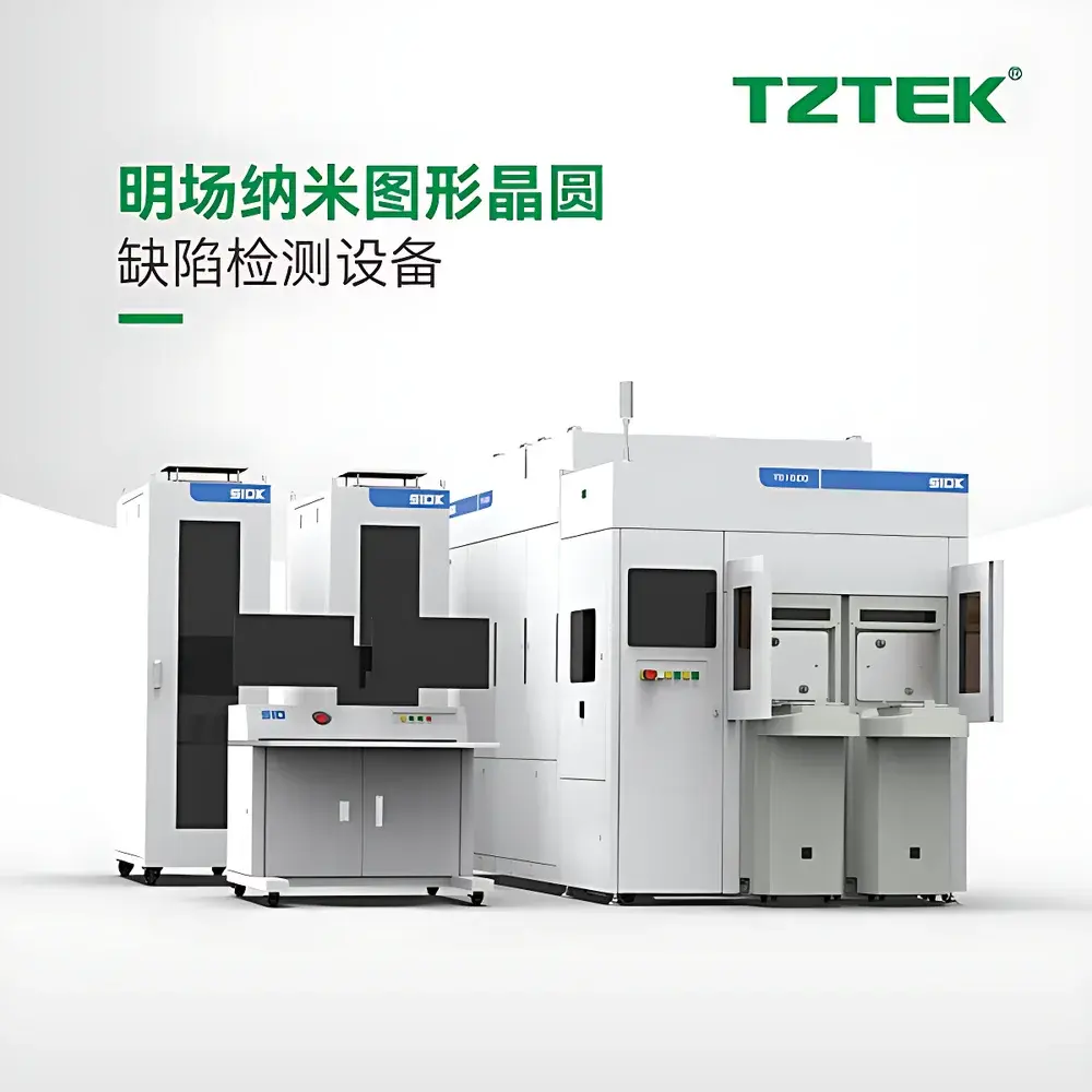
TZTEK TB Series Bright-Field Nanoscale Patterned Wafer Defect Inspection System
| Brand | TZTEK |
|---|---|
| Origin | Jiangsu, China |
| Manufacturer Type | Original Equipment Manufacturer (OEM) |
| Country of Origin | China |
| Model | TB Series |
| Instrument Category | Optical Patterned Wafer Defect Inspection System |
| Primary Application | Semiconductor Wafer Defect Detection |
| Supported Wafer Diameters | 200 mm (8-inch), 300 mm (12-inch) |
| Compliance | Designed for integration into semiconductor front-end and back-end process lines |
Overview
The TZTEK TB Series Bright-Field Nanoscale Patterned Wafer Defect Inspection System is an automated, wide-spectrum optical inspection platform engineered for high-precision defect detection on patterned semiconductor wafers. Utilizing bright-field illumination across multiple visible and near-UV wavelengths, the system captures high-resolution intensity contrast images of nanoscale device structures—enabling reliable identification of surface and near-surface anomalies including particles, scratches, bridging, missing patterns, micro-scratches, and lithographic residues. The TB Series is purpose-built for in-line process monitoring in both front-end-of-line (FEOL) and back-end-of-line (BEOL) fabrication environments, supporting technology nodes down to 28 nm and compatible with advanced patterning schemes such as double-patterning and self-aligned quadruple patterning (SAQP). Its modular optical architecture integrates high-numerical-aperture (NA) objectives, precision motion stages, and real-time focus tracking to maintain sub-micron spatial fidelity across full-wafer scans.
Key Features
- Multi-wavelength bright-field illumination optimized for contrast enhancement across diverse film stacks (e.g., SiN, SiO₂, low-k dielectrics, metal interconnects)
- Automated wafer handling with SEMI-compliant FOUP/SMIF interface support for 200 mm and 300 mm wafers
- Real-time adaptive focus control using through-the-lens (TTL) autofocus sensors to compensate for wafer warp and topography-induced defocus
- High-throughput scanning engine capable of >60 wafers per hour (WPH) at ≤100 nm pixel resolution for 300 mm wafers
- Proprietary signal processing pipeline incorporating multi-scale spatial filtering, dynamic background normalization, and local contrast optimization to maximize defect signal-to-noise ratio (SNR)
- Integrated defect review capability with programmable zoom and multi-angle illumination for rapid root-cause correlation
Sample Compatibility & Compliance
The TB Series supports standard silicon, SOI, and compound semiconductor wafers with diameters of 200 mm and 300 mm, accommodating thicknesses from 525 µm to 775 µm and warpage up to ±20 µm. It is compatible with industry-standard photomasks, reticles, and process layers including gate oxides, shallow trench isolation (STI), copper damascene, and advanced packaging substrates. The system complies with SEMI E10 (Specification for Definition and Measurement of Equipment Reliability, Availability, and Maintainability), SEMI E19 (Wafer Carrier Interface Standards), and ISO 9001:2015 quality management requirements. Its hardware and software architecture are designed to support GLP/GMP-aligned audit trails, user access control, and electronic signature functionality per FDA 21 CFR Part 11 when deployed in regulated manufacturing environments.
Software & Data Management
The TB Series runs on TZTEK’s proprietary inspection software suite, which provides a unified interface for recipe setup, scan execution, defect classification, and statistical process control (SPC) reporting. Defect data is stored in a relational database compliant with SQL standards, supporting ODBC connectivity for integration with factory automation systems (FDC, MES, APC). The classification module employs supervised machine learning models trained on labeled defect libraries—including SEM-verified ground truth—to enable real-time, rule-based and AI-assisted defect categorization (e.g., particle vs. pattern shift vs. etch residue). All software logs—including operator actions, parameter changes, and calibration events—are timestamped and cryptographically signed to meet traceability requirements for internal audits and external regulatory assessments.
Applications
- Pre- and post-lithography defect screening for critical layer verification
- In-line monitoring of CMP endpoint and post-CMP residue detection
- Mask shop defect verification on photomasks and pellicles
- Post-etch inspection for line-edge roughness (LER), bridging, and incomplete etch
- Advanced packaging inspection including redistribution layer (RDL) and bump array integrity checks
- Process window qualification and yield ramp-up support during technology transfer
FAQ
What wafer sizes does the TB Series support?
The system is configured for automated handling and inspection of 200 mm (8-inch) and 300 mm (12-inch) wafers.
Is the TB Series compatible with cleanroom Class 100 environments?
Yes—the mechanical design, material selection, and airflow management conform to ISO Class 5 (Class 100) cleanroom specifications per ISO 14644-1.
Does the system support integration with existing fab automation infrastructure?
Yes—it includes SECS/GEM communication protocols, CIM-compatible event reporting, and configurable OPC UA server endpoints for seamless MES/FDC interoperability.
Can the defect classification model be retrained with customer-specific defect types?
Yes—TZTEK provides a certified model training toolkit with secure data ingestion pipelines, enabling customers to extend classification taxonomy under controlled validation protocols.
What calibration standards are used for sensitivity verification?
The system supports NIST-traceable reference wafers with certified defect sizes (e.g., 80 nm–500 nm polystyrene latex spheres) and is validated per ASTM F2682–21 for optical defect detection sensitivity assessment.


