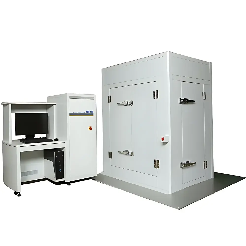

ULVAC-PHI PHI 710 Scanning Auger Nanoprobe
| Brand | ULVAC-PHI |
|---|---|
| Origin | Japan |
| Model | PHI 710 |
| Type | Scanning Auger Electron Spectrometer (AES) |
| SEM Resolution | ≤3 nm |
| AES Spatial Resolution | ≤8 nm (@20 kV, 1 nA) |
| Analyzer Geometry | Coaxial Cylindrical Mirror Analyzer (CMA) |
| Energy Resolution | 0.1% (high-resolution mode) |
| Beam Diameter | 20 nm (adjustable) |
| Ion Gun Sputtering Energy | 0.5 kV (standard configuration) |
| Software Suite | PHI SmartSoft-AES & MultiPak |
Overview
The ULVAC-PHI PHI 710 Scanning Auger Nanoprobe is a high-performance, ultra-high-vacuum (UHV) surface analysis instrument engineered for quantitative elemental and chemical state characterization at the nanoscale. Based on the physical principle of Auger electron spectroscopy (AES), the system detects core-level ionization-induced Auger electrons emitted from the top 0.5–3 nm of solid surfaces following primary electron beam excitation. Unlike X-ray photoelectron spectroscopy (XPS), AES offers superior spatial resolution due to its higher electron yield and favorable scattering cross-sections—making it uniquely suited for localized compositional mapping, interfacial reaction analysis, and thin-film depth profiling in technologically critical materials. The PHI 710 integrates a field-emission scanning electron microscope (SEM) column with a coaxial cylindrical mirror analyzer (CMA), enabling simultaneous high-resolution imaging and energy-filtered Auger signal acquisition without shadowing artifacts or angular sensitivity limitations.
Key Features
- Nanometer-scale spatial resolution: Achieves ≤3 nm SEM imaging resolution and ≤8 nm AES mapping resolution under standard operating conditions (20 kV, 1 nA), enabling precise targeting of sub-10 nm features such as gate oxides, metal silicide interfaces, or grain boundary segregants.
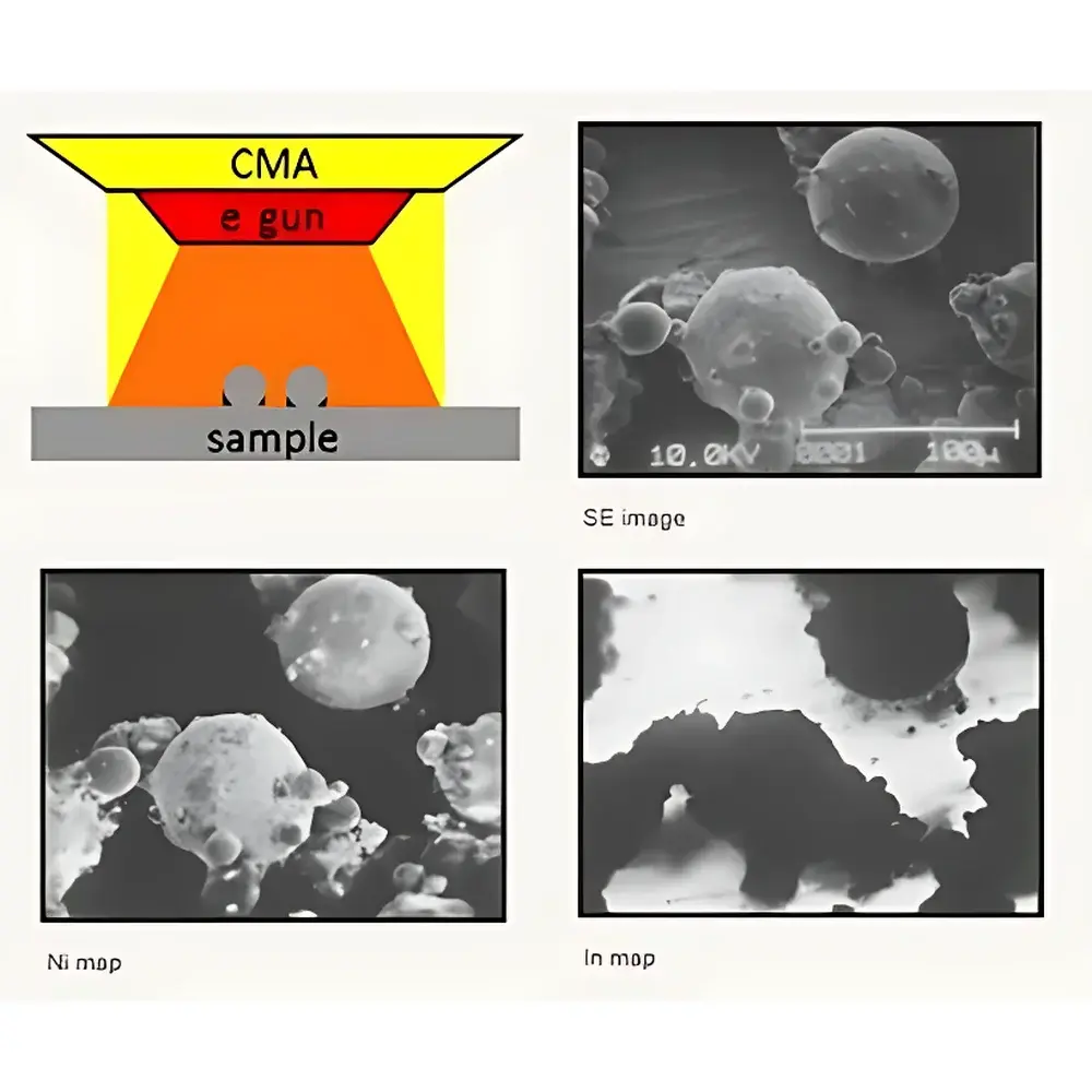
- Coaxial CMA geometry: The electron gun and analyzer share a common optical axis, eliminating line-of-sight obstructions and ensuring uniform collection efficiency across all sample orientations—including recessed regions, particle sidewalls, and inter-particle gaps—critical for representative surface interrogation of complex 3D microstructures.
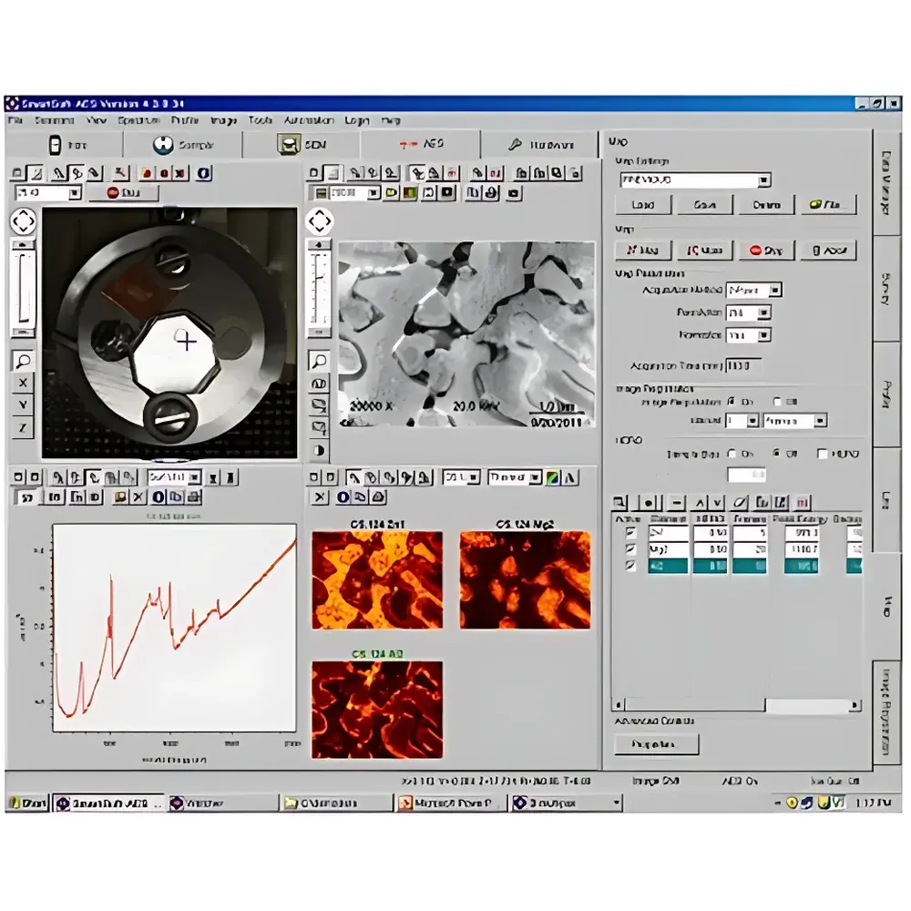
- Chemical-state-resolved imaging: Each pixel in an Auger map contains full spectral information; MultiPak software enables pixel-by-pixel least-squares spectral fitting (LLS) to distinguish chemically shifted Auger transitions (e.g., Si LMM peaks for elemental Si, SiOx, and NiSi), generating quantitative chemical-state distribution maps.
- High-energy-resolution depth profiling: With energy resolution configurable down to 0.1%, the system resolves fine structure in Auger peaks essential for identifying oxidation states, compound formation (e.g., Ni2Si vs. NiSi), and interdiffusion kinetics at buried interfaces.
- Integrated dual-software architecture: PHI SmartSoft-AES provides guided workflow automation for sample loading, region-of-interest definition, and parameter setup—reducing operator dependency and ensuring method reproducibility per ISO/IEC 17025 and GLP requirements. MultiPak delivers advanced post-processing including peak deconvolution, detection limit calculation (based on Poisson statistics), matrix correction (Shen-McClure algorithm), and image enhancement via principal component analysis (PCA).
Sample Compatibility & Compliance
The PHI 710 accommodates conductive and semi-conductive samples up to 25 mm in diameter, including wafers, TEM lamellae, fractured cross-sections, and catalytic nanoparticles. Non-conductive specimens require ultrathin (<2 nm) carbon coating to mitigate charging. All analyses are conducted under UHV conditions (base pressure ≤2×10⁻¹⁰ Torr), minimizing surface contamination during acquisition. The system complies with ASTM E1598 (Standard Practice for Auger Electron Spectroscopy), ISO 18118 (Surface chemical analysis — AES — terminology), and supports audit-ready data logging aligned with FDA 21 CFR Part 11 requirements when configured with electronic signature and secure user access controls.
Software & Data Management
PHI SmartSoft-AES enforces standardized operating procedures through step-based wizards—ensuring consistent vacuum pump-down sequences, beam alignment routines, and calibration checks prior to analysis. All raw spectra, maps, and depth profiles are stored in vendor-agnostic HDF5 format with embedded metadata (instrument parameters, date/time stamps, operator ID). MultiPak supports batch processing of multi-file datasets, automated report generation (PDF/HTML), and export to third-party platforms (e.g., MATLAB, Python via h5py). Spectral libraries include >2,400 reference Auger transitions curated from NIST SRD-20 and IUPAC-recommended databases, with built-in charge referencing and work-function correction tools.
Applications
- Semiconductor metrology: Interface diffusion quantification in CMOS gate stacks, identification of residual fluorine/carbon contaminants after etch, failure analysis of Cu/low-k interconnect delamination, and FIB-prepared device cross-section characterization.
- Advanced packaging: SnAgCu solder joint intermetallic compound (IMC) growth kinetics, under-bump metallization (UBM) integrity assessment, and void detection at die-attach interfaces.
- Magnetic recording media: Oxidation state mapping of CoCrPt alloy granular films, segregation analysis of Cr-rich grain boundaries, and thickness uniformity evaluation of Ru intermediate layers.
- Functional ceramics & coatings: Grain boundary segregation of Y in YSZ electrolytes, oxidation front propagation in thermal barrier coatings, and dopant distribution homogeneity in piezoelectric PZT thin films.
FAQ
What vacuum level is required for reliable Auger analysis?
Ultra-high vacuum (UHV) conditions ≤2×10⁻¹⁰ Torr are mandatory to prevent hydrocarbon adsorption and maintain surface cleanliness during acquisition.
Can the PHI 710 analyze insulating samples without conductive coating?
No—charging effects distort both SEM imaging and Auger peak positions; a ≤2 nm carbon or Au/Pd sputter coat is required for non-conductive materials.
How does the coaxial CMA improve quantitative accuracy compared to off-axis analyzers?
It eliminates angular dependence in electron collection efficiency, enabling uniform sensitivity across topographically complex surfaces and eliminating shadowing-induced quantification errors.
Is depth profiling possible with monolayer resolution?
While true monolayer sputtering is not achievable, combined with low-energy Ar+ ion beams (0.5–2 keV) and optimized sputter yields, the system achieves <0.3 nm effective depth resolution in optimized matrix-matched standards.
Does MultiPak support compliance with regulatory data integrity standards?
Yes—when deployed with PHI’s optional Audit Trail Module, MultiPak logs all user actions, parameter changes, and data modifications in immutable, time-stamped records compliant with 21 CFR Part 11 and EU Annex 11.