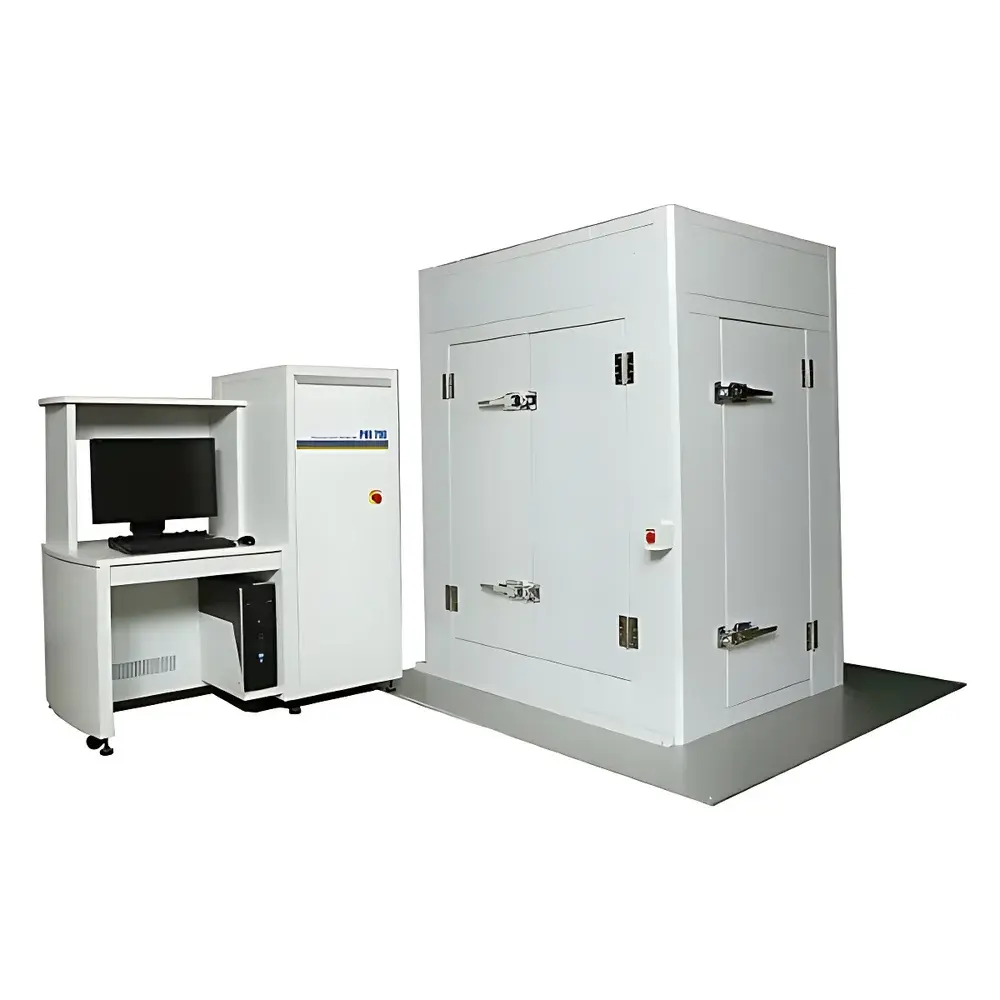
ULVAC-PHI PHI 710 Scanning Auger Nanoprobe
| Brand | ULVAC-PHI |
|---|---|
| Origin | Japan |
| Model | PHI 710 |
| Category | Imported Instrument |
| Vendor Type | Authorized Distributor |
| Pricing | Upon Request |
Overview
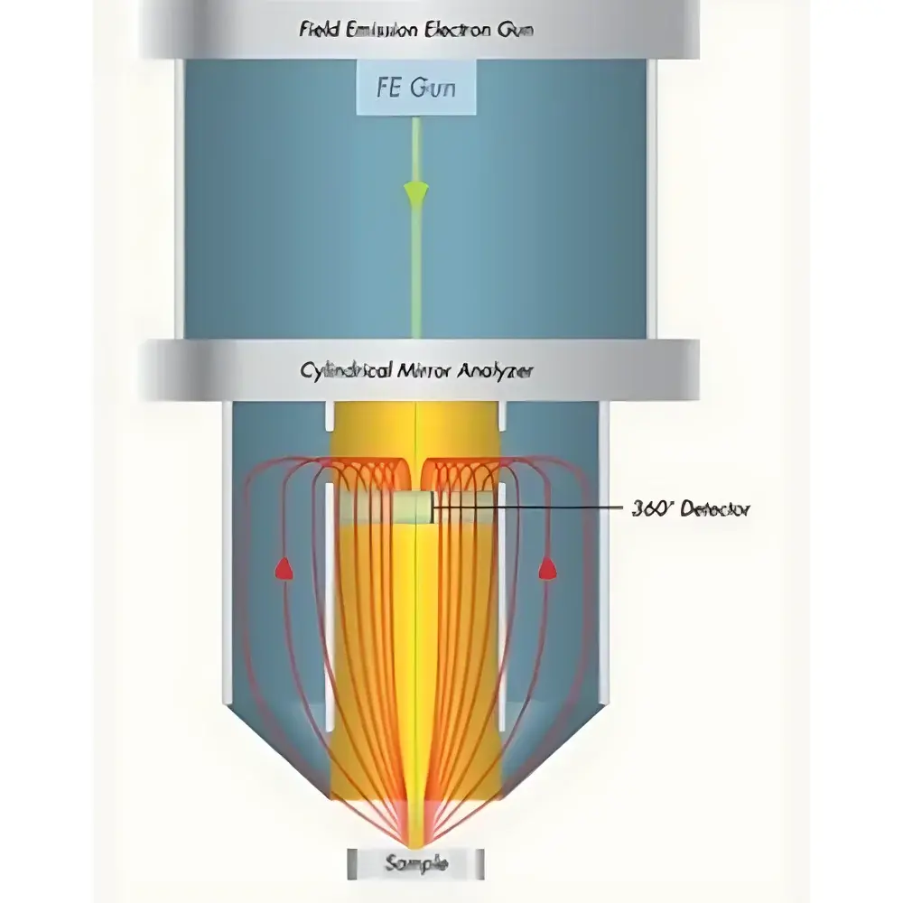
The ULVAC-PHI PHI 710 Scanning Auger Nanoprobe is a high-performance, ultra-high-vacuum (UHV) surface analysis instrument engineered for quantitative elemental and chemical state characterization at the nanoscale. It operates on the fundamental principle of Auger Electron Spectroscopy (AES), where a focused electron beam excites core-level electrons in the sample surface; the subsequent relaxation cascade emits Auger electrons whose kinetic energies are element-specific and chemically sensitive. Unlike conventional XPS or EDS, AES provides superior spatial resolution (<8 nm at 20 kV, 1 nA) and surface sensitivity (top 0.5–3 nm), making it indispensable for interface science, thin-film metrology, and failure analysis in advanced microelectronics and functional materials. The PHI 710 integrates a field-emission scanning electron microscope (SEM) with a coaxial cylindrical mirror analyzer (CMA), enabling simultaneous high-resolution imaging and spectroscopic mapping without geometric shadowing artifacts—critical for three-dimensional particle and grain boundary analysis.
Key Features
- Sub-3 nm SEM spatial resolution and ≤8 nm AES lateral resolution under standard operating conditions (20 kV, 1 nA), validated per ASTM E1508 and ISO 18118 standards for surface analysis instrumentation.
- Coaxial CMA geometry: Ensures uniform collection solid angle across all sample orientations, eliminating directional sensitivity and shadowing—essential for accurate quantification of irregular topographies and embedded interfaces.
- Dual-beam capability: Combines high-brightness Schottky field-emission electron source with optional integrated low-energy ion gun (0.1–5 keV) for controlled sputter depth profiling with sub-nanometer depth resolution.
- Energy resolution: Adjustable down to 0.1% of pass energy (e.g., 0.3 eV at 300 eV), enabling discrimination of subtle chemical shifts in Si, C, O, N, and transition metals—validated against NIST SRM 2100 and PHI-certified reference spectra.
- Integrated SmartSoft-AES software platform: Task-driven workflow with guided sample loading, region-of-interest definition, and parameter presetting—designed for compliance with GLP and GMP environments requiring audit-trail documentation per FDA 21 CFR Part 11.
Sample Compatibility & Compliance
The PHI 710 accommodates conductive and semi-conductive samples up to 25 mm in diameter and 10 mm in height, including wafers, TEM lamellae, fractured cross-sections, and catalytic nanoparticles. Non-conductive specimens require ultra-thin carbon coating (<2 nm) to mitigate charging, verified via charge neutralization stability tests. All vacuum chambers maintain base pressures <2×10⁻¹⁰ Torr (measured by Bayard-Alpert gauge), meeting UHV requirements specified in ISO 14644-1 Class 1 cleanroom protocols for surface-sensitive analysis. The system complies with IEC 61000-6-3 (EMC) and IEC 61010-1 (safety), and supports traceable calibration using certified reference materials traceable to NIST and BAM standards.
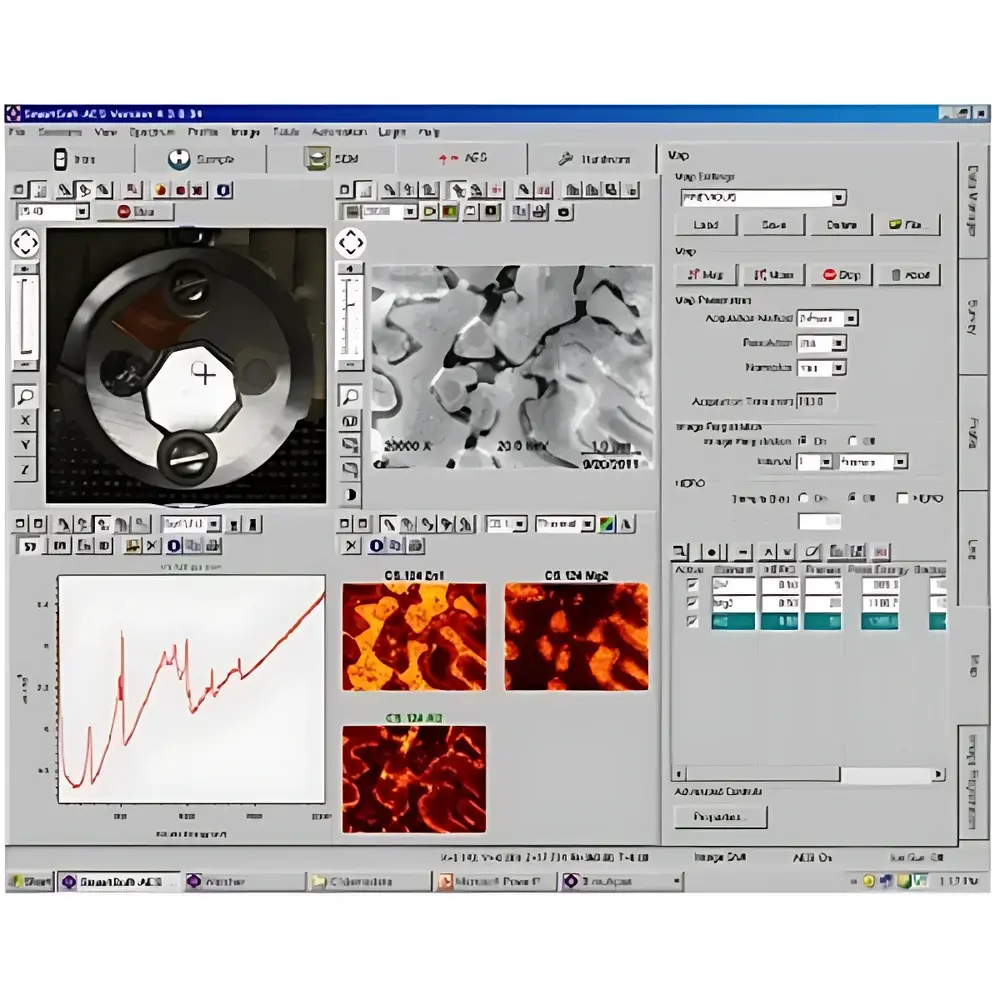
Software & Data Management
PHI MultiPak serves as the core data processing suite, supporting full spectral deconvolution, least-squares fitting (LLS), chemical-state mapping, and quantitative depth profiling. Its built-in Auger database includes over 1,200 reference spectra for elemental and compound identification, aligned with the PHI Auger Handbook and the Surface Science Spectra (SSS) database. All raw and processed datasets are stored in vendor-neutral HDF5 format with embedded metadata (instrument parameters, vacuum history, operator ID, timestamp), enabling interoperability with third-party platforms such as Thermo Scientific Avantage and CasaXPS. Audit trails—including user actions, parameter modifications, and report generation—are automatically logged and exportable for regulatory submissions.
Applications
- Semiconductor manufacturing: Interface diffusion kinetics in gate stacks (e.g., SiO₂/SiNₓ/HfO₂), metal silicide formation (NiSi, CoSi₂) at contact interfaces, FIB-induced damage assessment, and residue identification post-etch/clean processes.
- Advanced displays: Thin-film transistor (TFT) channel composition verification, ITO/oxide semiconductor interfacial oxidation states, and defect-associated contamination mapping in OLED encapsulation layers.
- Magnetic storage: Multilayer CoCrPt-based media surface oxidation, NiFe read head corrosion products, and grain boundary segregation in perpendicular recording media.
- Structural materials: Grain boundary embrittlement studies (e.g., S, P segregation in steels), thermal barrier coating interdiffusion (YSZ/NiCrAlY), and passive film composition analysis on stainless steels and Ni-based superalloys.
FAQ
What is the minimum detectable concentration for AES on the PHI 710?
Typical detection limits range from 0.1–0.5 at.% for most elements under optimized acquisition conditions (≥10⁴ counts per peak, 300 eV pass energy), depending on elemental mass, matrix effects, and surface roughness.
Can the PHI 710 perform depth profiling on insulating films?
Yes—with charge compensation via low-energy electron flood gun and adjustable ion beam incidence angle, enabling stable profiling of SiO₂, Al₂O₃, and polymer dielectrics up to 200 nm depth.
Is the system compatible with in-situ fracture stages?
Optional cryogenic or room-temperature in-situ brittle fracture stages allow UHV transfer of freshly exposed surfaces directly into the analysis chamber, preserving native surface chemistry per ASTM E1188.
How does the coaxial CMA improve quantitative accuracy compared to off-axis analyzers?
By eliminating angular dependence in electron collection efficiency, the CMA ensures uniform sensitivity across tilted, curved, or particulate surfaces—reducing systematic errors in relative sensitivity factor (RSF)-based quantification by up to 35% versus conventional designs.
Does MultiPak support automated phase identification in multiphase alloys?
Yes—through integrated cluster analysis and principal component mapping (PCA), MultiPak enables unsupervised segmentation of complex microstructures (e.g., duplex stainless steels, Ti-6Al-4V) based on Auger spectral variance.