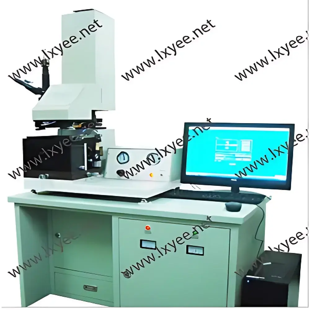

WUXI CAS PHOTONICS URE-2000S/25A UV Double-Side Mask Aligner
| Brand | WUXI CAS PHOTONICS INC |
|---|---|
| Origin | Sichuan, China |
| Model | URE-2000S/25A |
| Exposure Area | 6-inch wafer |
| Exposure Wavelength | 365 nm (i-line) |
| Irradiance | >25 mW/cm² |
| Resolution | 1 µm |
| Alignment Accuracy | ±2 µm (double-side, 0.8 mm substrate thickness), ±0.8 µm (single-side) |
| Illumination Uniformity | ≤2.5% (Φ100 mm), ≤4% (Φ150 mm) |
| Mask-to-Wafer Motion Range | X: ±5 mm, Y: ±5 mm, Θ: ±6° |
| Mercury Lamp | 350 W DC, imported (OSRAM) |
| Collimation Angle | 3.5° |
| Maximum Photoresist Thickness | 350 µm (SU-8, under specified process conditions) |
| Dimensions (L×W×H) | 1300 × 900 × 1800 mm |
Overview
The WUXI CAS PHOTONICS URE-2000S/25A is a high-precision, manually loaded UV double-side mask aligner engineered for academic research, prototyping, and low-to-medium volume semiconductor fabrication. It operates on the principle of contact/proximity photolithography using i-line (365 nm) radiation from a stabilized 350 W DC mercury arc lamp. The system delivers collimated, uniform illumination across a 6-inch (152 mm) diameter field via a multi-element fly’s-eye lens array and cold-light elliptical reflector architecture—minimizing thermal load on masks and substrates while preserving critical dose fidelity. Its dual-sided alignment capability enables simultaneous top- and bottom-surface pattern registration with sub-micron repeatability, supporting applications such as through-silicon via (TSV) interconnect definition, MEMS device fabrication, and symmetric microstructure patterning on transparent or opaque wafers up to 2 mm thick.
Key Features
- Double-side alignment architecture with independent optical paths: top-side binocular dual-field microscope (400× optical / 800× combined optical-electronic magnification) and bottom-side CCD-based imaging system with adjustable objective spacing (10–148 mm)
- Three-tier magnification optics: interchangeable 4×, 10×, and 20× objectives and eyepieces; vertical dual-CCD alignment subsystem with 0.65–4.5× continuous optical zoom and lateral oblique illumination for edge contrast enhancement
- Digital gap control: programmable alignment and exposure gaps with sensor-based contact pressure feedback ensuring consistent mechanical reproducibility during soft/hard contact modes
- Modular interface support: standardized mechanical and pneumatic interfaces for optional proximity gap control (5–50 µm) and nanoimprint lithography (NIL) integration
- Thermally stable optical train: cold-light reflectors, i-line bandpass filter, and dual collimating lenses reduce infrared radiation and chromatic aberration, enabling high-fidelity 1 µm resolution patterning in SU-8 and standard g/i-line resists
- Full vacuum chuck system with four dedicated carrier stages (2″, 3″, 4″, 6″) and four mask holders (3″–7″), compatible with substrates ranging from 0.1 mm to 2.0 mm thickness
Sample Compatibility & Compliance
The URE-2000S/25A accommodates rigid and semi-rigid substrates including silicon, glass, quartz, sapphire, and polymer films. Its mechanical design conforms to ISO 14644-1 Class 5 cleanroom operational guidelines when used with appropriate environmental controls. While not certified for GMP production environments, its traceable digital exposure control (dose- and time-based modes), calibrated irradiance monitoring, and audit-ready manual logbook structure support GLP-compliant R&D workflows. The system meets CE electromagnetic compatibility (EMC) requirements per EN 61326-1 and laser safety standards for Class 3B UV sources (IEC 60825-1), with interlocked enclosure and shutter mechanisms preventing unintended exposure.
Software & Data Management
Control is executed via an embedded single-board computer running real-time firmware with a dedicated 21-inch industrial LCD HMI. Exposure parameters—including dose (mJ/cm²), time (s), lamp warm-up status, and gap settings—are stored locally with timestamped logs exportable via USB. The system supports external PC integration for advanced image analysis (e.g., overlay error quantification via cross-correlation algorithms) and batch recipe management. Though no native FDA 21 CFR Part 11-compliant electronic signature module is included, the architecture permits third-party validation of data integrity and user access logs in regulated development labs.
Applications
- Fabrication of MEMS sensors requiring precise front-to-back alignment (e.g., pressure transducers, accelerometers)
- Research-scale TSV patterning and redistribution layer (RDL) definition on thinned wafers
- Microfluidic device prototyping on PDMS, PMMA, and glass substrates
- Optical grating and photonic crystal mask alignment for university cleanroom facilities
- Low-cost back-end-of-line (BEOL) process development for compound semiconductors and flexible electronics
- Education and training in photolithography fundamentals, including diffraction-limited resolution studies and proximity effect characterization
FAQ
What wafer sizes does the URE-2000S/25A support?
It accepts 2-inch, 3-inch, 4-inch, and 6-inch wafers (diameter), with thickness ranging from 0.1 mm to 2.0 mm for double-side alignment.
Is the system compatible with standard i-line photoresists?
Yes—it is optimized for g-line and i-line resists (e.g., AZ series, SU-8, Shipley Microposit), delivering verified 1 µm resolution with appropriate process tuning.
Does the aligner include vacuum and compressed air sources?
Yes—a certified oil-free vacuum pump and ultra-quiet air compressor are supplied as standard equipment, eliminating need for facility-supplied utilities.
Can the exposure dose be controlled by energy rather than time?
Yes—both timed exposure and dose-controlled (mJ/cm²) modes are available, with real-time UV intensity feedback from integrated radiometric monitoring.
Are calibration certificates provided for optical and mechanical subsystems?
Factory calibration reports for lamp output stability, illumination uniformity, and alignment stage repeatability are included; NIST-traceable recalibration services are available upon request.


