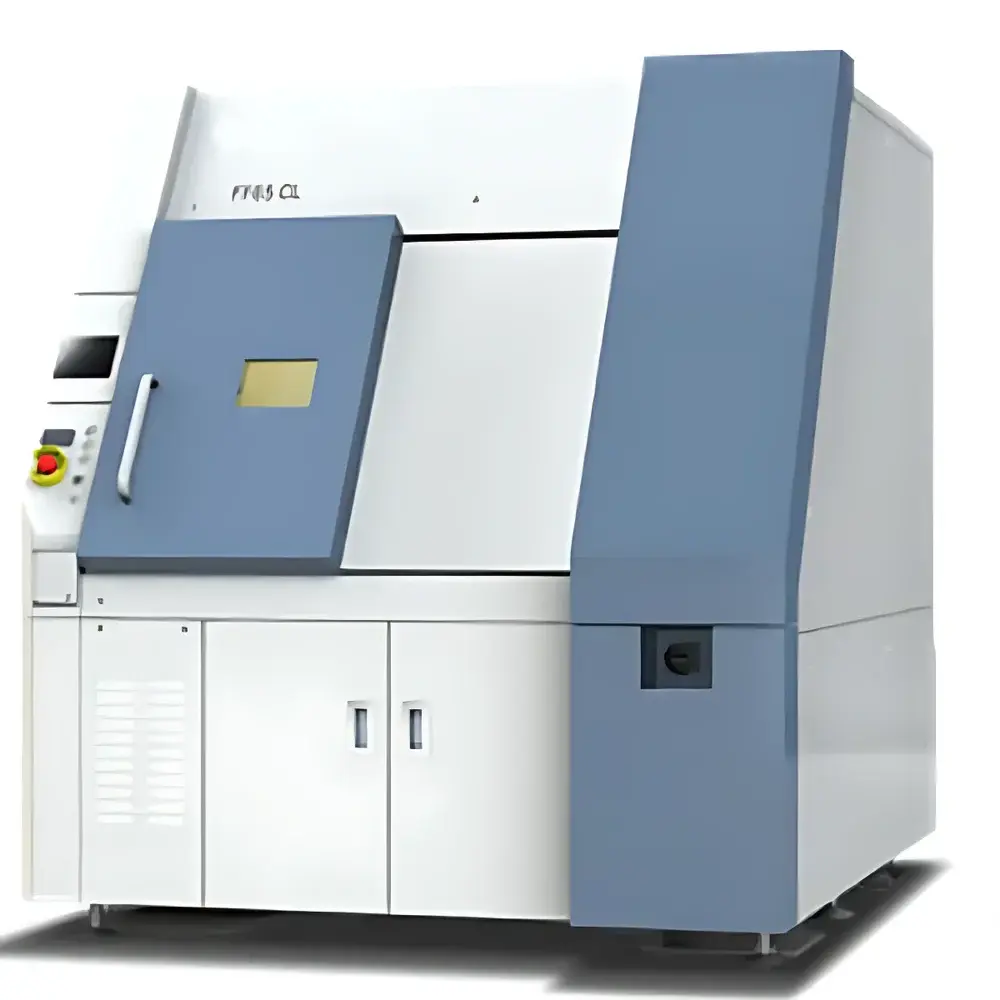
YXLON FF65 CL High-Resolution 3D X-ray Industrial Micro-CT System
| Brand | YXLON |
|---|---|
| Origin | Germany |
| Model | FF65 CL |
| Detector Type | Image Intensifier-Based Laminography Detector |
| Sample Diameter | 795 mm |
| Sample Height | 20 mm |
| Max Sample Weight | 2 kg |
| System Dimensions | 1760 × 2000 × 2000 mm |
| CT Mode | Super-High-Resolution Computed Laminography (CL) |
| Manipulation | Super-Precise Manipulator with Active Anti-Vibration System |
| Vacuum Sample Hold Mechanism | Integrated |
| Effective Detection Area | 510 × 610 mm |
| X-ray Source | Next-Generation Nanofocus Tube (≤ 300 nm focal spot) |
Overview
The YXLON FF65 CL is a purpose-engineered industrial micro-computed laminography (CL) system designed for non-destructive, high-fidelity 3D inspection of advanced semiconductor packages, including 3D ICs, flip-chip assemblies, wafer-level packaging (WLP), and MEMS sensors. Unlike conventional cone-beam micro-CT, computed laminography employs oblique acquisition geometry—rotating both the sample and detector around a tilted axis—to maintain optimal magnification and geometric sharpness for planar, layered structures up to 795 mm in diameter. This architecture eliminates parallax-induced blurring and enables sub-300 nm feature resolvability in critical interconnect regions such as solder bumps, copper pillars, and filled through-silicon vias (TSVs). The system integrates a next-generation nanofocus X-ray source (≤ 300 nm focal spot), vacuum-assisted precision sample fixation, and active vibration isolation—ensuring mechanical stability during long-duration, high-magnification scans required for statistical process control (SPC) and failure analysis (FA) in high-volume manufacturing environments.
Key Features
- Super-high-resolution computed laminography (CL) mode optimized for planar electronics—delivering isotropic voxel resolution down to <300 nm in reconstructed volumes without geometric distortion.
- Integrated vacuum-based sample holding stage with real-time warpage compensation—maintains flatness and positional fidelity for thin wafers (≤ 20 mm height) and large-area substrates (up to 795 mm diameter).
- Active anti-vibration manipulator platform with sub-micron repeatability—engineered for stable acquisition across multi-hour automated scan sequences.
- Dual-mode imaging capability: high-throughput top-down 2D AXI (Automated X-ray Inspection) and quantitative 3D CL reconstruction within a single unified workflow.
- Intuitive graphical user interface (GUI) supporting drag-and-drop program creation for multi-point, multi-angle, and multi-threshold defect detection routines—compliant with semiconductor equipment communication standards (SECS/GEM).
- On-the-fly background calibration monitoring—automatically tracks detector gain drift, beam hardening, and source intensity variation to preserve measurement traceability over time.
Sample Compatibility & Compliance
The FF65 CL accommodates full-wafer formats (200 mm to 450 mm), panel-level substrates (up to 510 × 610 mm active area), and packaged modules (e.g., fan-out wafer-level packages, 2.5D/3D SiP). Its mechanical design conforms to SEMI S2/S8 safety guidelines and supports integration into Class 100 cleanroom environments. Data acquisition and reconstruction workflows are structured to support audit-ready documentation per ISO/IEC 17025, ASTM E2737 (Standard Practice for Computed Tomography), and IEC 62209-2 (for RF-related package integrity verification). All measurement metadata—including source parameters, geometric calibration coefficients, and reconstruction kernels—is embedded in DICOM-CT and HDF5 export formats, ensuring compatibility with enterprise MES/QMS platforms and enabling GLP/GMP-aligned reporting.
Software & Data Management
YXLON’s proprietary ctAnalyzer software provides full-stack control—from acquisition protocol definition and real-time projection preview to GPU-accelerated FDK and iterative reconstruction (SART, OS-SART). Defect classification uses rule-based and supervised ML models trained on labeled semiconductor defect libraries (voids, cracks, bridging, insufficient fill). Quantitative outputs include volumetric porosity, bump coplanarity deviation (µm), TSV fill ratio (%), and interfacial delamination surface area (mm²)—all traceable to NIST-traceable phantoms. Raw projections and reconstructed volumes are stored with SHA-256 checksums; software logs comply with FDA 21 CFR Part 11 requirements for electronic records and signatures, including full operator audit trails, parameter change history, and locked result archives.
Applications
- Automated inline qualification of solder bump height, shape, and co-planarity in 3D stacked ICs.
- Non-destructive metrology of copper pillar height and die tilt in advanced flip-chip interconnects.
- Void detection and quantification in underfill and molding compounds—correlated with thermal cycling reliability data.
- Failure analysis of TSVs and redistribution layers (RDLs) post-packaging or after accelerated stress testing (HAST, TC).
- Process window validation for electroplating, reflow, and bonding steps—using statistical voxel-based density mapping across production lots.
- Reference-free dimensional verification of MEMS cavity depths and diaphragm thickness uniformity.
FAQ
What distinguishes computed laminography (CL) from conventional micro-CT for semiconductor inspection?
Computed laminography eliminates cone-beam artifacts inherent in standard micro-CT when imaging flat, layered samples—by acquiring projections along a tilted axis, it preserves spatial coherence across large fields-of-view while maintaining sub-micron resolution at depth.
Does the FF65 CL support automated defect classification for high-volume production?
Yes—the system integrates configurable rule-based thresholds and optional supervised machine learning models trained on customer-specific defect sets, with output reports formatted for direct ingestion into factory MES systems.
How is measurement stability maintained over extended operational periods?
Continuous background calibration monitors detector response and X-ray source output; geometric recalibration is performed automatically before each batch using embedded fiducial markers and laser interferometric stage verification.
Can the system be integrated into a fully automated fab environment?
It supports SECS/GEM communication protocols, SMEMA handshaking, and Ethernet/IP connectivity—enabling seamless integration with automated material handling systems (AMHS) and centralized process control infrastructure.
Is raw projection data accessible for third-party reconstruction or custom algorithm development?
Yes—unprocessed projections are exported in TIFF or HDF5 format with full metadata, including source-to-detector geometry, exposure timing, and filter configuration, enabling external research or proprietary pipeline integration.


