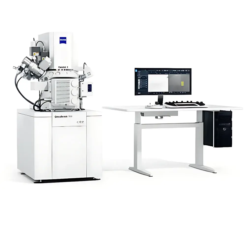
ZEISS Crossbeam 330 DualBeam Focused Ion Beam Scanning Electron Microscope
| Brand | ZEISS |
|---|---|
| Origin | Germany |
| Model | Crossbeam 330 DualBeam SEM/FIB |
| Configuration | Integrated electron column + gallium liquid metal ion source (LMIS) FIB column |
| Vacuum system | Differential pumping with cold trap and turbomolecular pumps |
| Stage | Motorized 5-axis precision stage with ±90° tilt, 360° rotation, sub-micron repeatability |
| Detector suite | In-lens SE, ETSE, STEM, BSE, EDS-compatible |
| Optional integration | X-ray tomography (XRM) correlation module |
Overview
The ZEISS Crossbeam 330 is a high-performance dual-beam platform that co-integrates a field-emission scanning electron microscope (FE-SEM) and a focused gallium ion beam (FIB) within a single, ultra-stable vacuum chamber. Engineered for correlative nanoscale analysis and precision sample manipulation, it operates on the principle of simultaneous or sequential electron imaging and ion-induced sputtering—enabling real-time observation of milling, deposition, and cross-sectioning processes at sub-10 nm resolution. Its non-magnetic objective lens design eliminates magnetic field interference, permitting direct imaging and milling of ferromagnetic, insulating, or beam-sensitive specimens without conductive coating or complex charge compensation protocols. The in-column deceleration technology ensures low-voltage electron imaging (<1 kV) with high surface sensitivity and minimal charging—critical for polymers, ceramics, and biological composites.
Key Features
- Gemini II electron optical system: Delivers sub-nanometer resolution at 1 kV and <0.7 nm at 15 kV, with high signal-to-noise ratio across diverse material classes.
- High-brightness Ga⁺ liquid metal ion source: Provides stable, high-current FIB operation (up to 60 nA) with sub-10 nm probe size, enabling rapid trenching, lamella thinning, and site-specific ablation.
- In-chamber real-time monitoring: Electron imaging during ion milling allows dynamic process control—no need to interrupt FIB operation for intermediate SEM checks.
- Automated TEM lamella preparation workflow: Guided by ZEISS SmartSEM software, including auto-alignment, fiducial marker placement, iterative thinning, and final polishing—all traceable and repeatable per GLP-compliant logs.
- Modular detector architecture: Supports in-lens secondary electron (SE), Everhart-Thornley (ETSE), backscattered electron (BSE), and STEM-in-SEM modes; fully compatible with energy-dispersive X-ray spectroscopy (EDS) systems for elemental mapping.
Sample Compatibility & Compliance
The Crossbeam 330 accommodates samples up to 150 mm in diameter and 50 mm in height, with compatibility extending to conductive metals, semiconductors, oxides, geological thin sections, battery cathode/anode composites, and hydrated or cryo-fixed biological tissues (when paired with optional cryo-transfer). Its differential vacuum architecture maintains <1×10⁻⁷ mbar in the electron column and <5×10⁻⁵ mbar in the FIB column—meeting ISO 14644-1 Class 4 cleanroom requirements for contamination-sensitive workflows. System operation complies with IEC 61000-6-3 (EMC) and IEC 61000-6-4 (immunity); software audit trails satisfy FDA 21 CFR Part 11 and EU Annex 11 requirements for regulated environments.
Software & Data Management
Controlled via ZEISS SmartSEM software v8.x, the platform supports scriptable automation (Python API), batch processing, and multi-user role-based access. All imaging, milling, and alignment parameters are timestamped and stored in a relational database with SHA-256 hash integrity verification. Raw data export adheres to open formats (TIFF, HDF5, EMDB-compatible metadata), facilitating integration with third-party reconstruction tools (e.g., Avizo, Dragonfly) and laboratory information management systems (LIMS). Full electronic records—including operator ID, session log, and instrument calibration status—are retained for ≥30 years per internal archive policy.
Applications
- Advanced materials: Quantitative 3D reconstruction of grain boundaries, porosity networks, and phase distribution in Ni-based superalloys and MAX-phase ceramics.
- Electronics & semiconductors: Circuit edit, failure analysis (FA), and through-silicon via (TSV) cross-sectioning with <5 nm positional accuracy.
- Energy storage: Correlative FIB-SEM/XRM workflows for locating and extracting individual particles from Li-ion battery electrodes; subsequent TEM analysis of solid-electrolyte interphase (SEI) morphology.
- Geosciences: Nanoscale characterization of shale matrix permeability, fluid inclusion geometry, and diagenetic mineral replacement textures.
- Life sciences: Targeted extraction of organelles from frozen-hydrated cells for cryo-TEM, enabled by low-kV electron imaging and minimized ion beam damage.
FAQ
Does the Crossbeam 330 support in-situ gas injection for platinum or carbon deposition?
Yes—equipped with a multi-channel gas injection system (GIS) compatible with Pt, C, SiO₂, and W precursors, enabling precise nanoscale circuit repair and protective layer deposition.
Can it be integrated with an external X-ray microtomography system?
Yes—via ZEISS CorrSight interface, enabling automated coordinate transfer between XRM volumetric datasets and FIB-SEM target coordinates for true 3D correlative analysis.
What level of training and service support is provided?
ZEISS offers factory-certified installation, application-specific training (including TEM lamella prep and 3D tomography), and 24/7 remote diagnostics with on-site response SLAs aligned to ISO/IEC 17025-accredited service centers.


