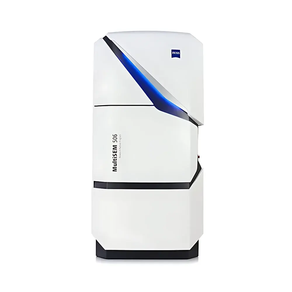
ZEISS MultiSEM High-Throughput Parallel-Beam Scanning Electron Microscope
| Brand | ZEISS |
|---|---|
| Origin | Germany |
| Model | MultiSEM |
| Electron Beam Configuration | Hexagonal array of 91 beams |
| Landing Energy Range | 1.0–3.0 kV |
| Average Resolution (all beams) | ≤ 3.5 nm @ 1.0 / 1.5 / 3.0 kV |
| Resolution Uniformity | ≤ ±1 nm @ 1.0 / 1.5 / 3.0 kV and 12 µm pitch |
| Beam Pitch Options | 12 µm (standard), 15 µm (optional) |
| Pitch Uniformity | ≤ ±1% |
| Field of View (hexagonal long axis) | 132 µm (12 µm pitch) or 165 µm (15 µm pitch) |
| Per-Beam Current | ≥ 570 pA |
| Total Probe Current | ≥ 52 nA |
| Current Uniformity | ≤ +10% |
| Electron Source | Schottky field-emission gun |
| Filament Current Stability | ≤ 1% per hour |
| Beam Blanking | Electrostatic |
| Working Distance | 1.4 mm |
| Detector System | High-efficiency multi-channel secondary electron detection with projection optics |
| Maximum Scan Rate per Beam | 20 MHz |
| Pixel Size Range | 2–20 nm (12 µm pitch) |
| Image Stitching | Fully automated, 91-subimage hexagonal tiling with adjustable overlap |
| Stage Type | Precision stepper stage |
| Stage Travel (X/Y/Z) | 100 / 100 / 30 mm |
| Stage Repeatability (XY) | ≤ ±3 µm |
| Sample Exchange Time (with exchange chamber) | ≤ 5 min |
| Sample Dimensions (max) | 100 × 100 mm² (XY), ≤ 30 mm height, ≤ 0.2 kg mass, surface flatness ≤ 500 nm P–P over 100 µm |
| Vacuum System | Turbo-molecular pump (>260 L/s) + oil-free scroll pump |
| Control Hardware | ≥4-core 64-bit CPU, ≥32 GB DDR RAM, ≥1 TB HDD, dual 1 Gbit Ethernet |
| OS | Windows 10 (64-bit) |
| Image Acquisition Nodes | 12 rack-mounted computers (≥4-core 64-bit CPU, ≥32 GB DDR3, 1 Gbit + 10 Gbit Ethernet) |
| Software Platform | ZEN core interface with Shuttle & Find, API for custom workflow integration, distributed acquisition database, automated focus/astigmatism/detector balancing, ROI-driven auto-sectioning, continuous serial sectioning workflows, real-time system health monitoring (vacuum, alignment, beam stability) |
Overview
The ZEISS MultiSEM is a high-throughput, parallel-beam scanning electron microscope engineered for nanoscale imaging at unprecedented speed and scalability. Unlike conventional single-beam SEMs, the MultiSEM employs a fixed hexagonal array of 91 independently controlled electron beams—each generated from a common Schottky field-emission source and focused through a shared condenser and objective lens system. This architecture leverages Couette-type beam separation and electrostatic blanking to enable true parallel acquisition across a large field of view. Operating at landing energies between 1.0 and 3.0 kV, the system delivers an average resolution of ≤3.5 nm across all 91 beams, with tight uniformity (≤±1 nm) critical for quantitative correlative analysis. Designed for unattended, 24/7 operation in industrial QA/QC labs and academic core facilities, the MultiSEM bridges the gap between macro-scale sample context and nanoscale structural detail—enabling full-surface imaging of specimens up to 100 × 100 mm² without mechanical repositioning or stitching artifacts.
Key Features
- 91 parallel electron beams arranged in a precision hexagonal lattice, enabling simultaneous scanning of discrete sub-regions
- Per-beam scan rates up to 20 MHz, supporting pixel dwell times compatible with high signal-to-noise secondary electron (SE) detection
- Integrated projection optics and multi-channel SE detectors optimized for collection efficiency and spatial fidelity at low kV
- Automated real-time beam alignment, astigmatism correction, focus optimization, and detector gain balancing
- Distributed acquisition architecture: 12 dedicated image nodes synchronized via deterministic 10 Gbit Ethernet, ensuring scalable throughput >1 TB/hour at 4 nm pixel size
- Robust vacuum architecture with active pressure monitoring, turbo-molecular pumping (>260 L/s), and oil-free backing—maintaining ≤1 × 10⁻⁵ mbar during continuous operation
- High-precision stepper stage with 100 mm × 100 mm travel, ≤±3 µm repeatability, and <5-minute sample exchange via load-lock chamber
Sample Compatibility & Compliance
The MultiSEM accommodates samples up to 100 × 100 mm² in planar dimension, 30 mm in height, and 0.2 kg in mass—subject to surface flatness ≤500 nm peak-to-peak over any 100 µm segment. Conductive coating is recommended for non-conductive specimens; carbon or Au/Pd sputtering protocols are fully compatible. The system meets ISO 14644-1 Class 5 cleanroom operational requirements when installed with appropriate environmental controls. Vacuum interlocks, beam shutdown protocols, and hardware-enforced dose limits align with IEC 61000-6-2/6-4 electromagnetic compatibility standards. Data integrity features—including audit-trail logging of all acquisition parameters, user actions, and calibration events—support compliance with GLP and GMP frameworks. While not FDA-cleared as a medical device, its traceable metrology and version-controlled software architecture facilitate 21 CFR Part 11 readiness when deployed in regulated biotech or materials R&D environments.
Software & Data Management
MultiSEM is controlled exclusively through ZEISS ZEN software—a unified platform extending the proven architecture from ZEISS optical microscopy into the SEM domain. ZEN provides a graphical workflow builder for ROI-based auto-sectioning, serial block-face imaging, and batch-acquisition scheduling. The Shuttle & Find function enables coordinate-preserving transfer between optical microscopes, single-beam SEMs, or light-sheet systems—critical for multimodal correlation. A documented RESTful API supports integration with LIMS, MES, and Python-based analysis pipelines (e.g., scikit-image, napari). All acquired images are stored in a distributed, metadata-rich database with embedded TIFF/OME-TIFF export, hierarchical tagging, and configurable retention policies. System performance metrics—including vacuum status, beam current drift, stage positional error, and detector saturation—are continuously logged and visualized in real time, enabling predictive maintenance and root-cause analysis of image quality deviations.
Applications
The MultiSEM excels in applications demanding statistical relevance through large-area, high-resolution coverage: semiconductor wafer defect review across full 300 mm substrates; 3D reconstruction of neural tissue via serial section TEM/SEM correlation; failure analysis of battery electrode microstructures over cm² domains; quality control of additive-manufactured metal parts including pore distribution mapping; and high-content screening of cultured cell monolayers on structured substrates. Its ability to acquire >1 TB/hour of calibrated, georeferenced SEM data makes it particularly suited for digital twin development in advanced manufacturing and for training deep learning models requiring ground-truth nanoscale annotations across heterogeneous material classes.
FAQ
How does the MultiSEM achieve higher throughput than conventional SEMs?
It uses 91 synchronized electron beams scanning in parallel across adjacent sub-fields—eliminating the serial raster delay inherent in single-beam systems while preserving nanoscale resolution and signal fidelity.
Is the system capable of automated long-duration acquisitions?
Yes. With full hardware redundancy, vacuum integrity monitoring, and self-diagnostic software, the MultiSEM is rated for unattended operation over 168-hour cycles under controlled lab conditions.
Can ZEN software be extended for custom image analysis?
Absolutely. The ZEN API provides access to raw detector streams, stage coordinates, and beam parameters—enabling integration with MATLAB, Python, or commercial AI inference engines.
What level of operator expertise is required for routine operation?
Minimal. Automated alignment, focus, and contrast routines reduce startup time to <5 minutes; most users achieve proficiency within one training day.
Does the system support energy-dispersive X-ray spectroscopy (EDS)?
Not natively. The MultiSEM is optimized for high-speed SE imaging; EDS integration requires external detector coupling and is evaluated on a case-by-case basis for specific application workflows.


