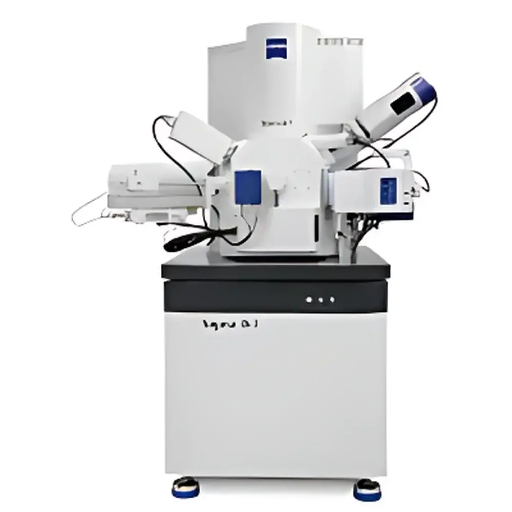

ZEISS Sigma 360 8-Inch Full-Wafer Electron Beam Inspection System
| Brand | ZEISS |
|---|---|
| Origin | Germany |
| Model | Sigma 360 |
| Wafer Handling | Full 200 mm (8-inch) diameter |
| Imaging Mode | Field Emission Scanning Electron Microscopy (FE-SEM) |
| Primary Application | Semiconductor Process Defect Inspection & CD Metrology |
| Vacuum System | Differential pumping with cold trap |
| Stage Type | Motorized polar-coordinate stage with collision-avoidance logic |
| Detector Configuration | In-lens EsB, SE2, and STEM-in-SEM options |
| Operating Voltage Range | 0.1–30 kV |
| Resolution | ≤1.0 nm @ 1 kV (in-lens SE mode) |
| Software Platform | SmartSEM Engineering Edition with wafer map navigation and recipe-driven automation |
Overview
The ZEISS Sigma 360 8-Inch Full-Wafer Electron Beam Inspection System is a purpose-engineered field emission scanning electron microscope (FE-SEM) platform optimized for high-throughput, high-fidelity defect review and critical dimension (CD) metrology on 200 mm (8-inch) semiconductor wafers. Unlike conventional SEMs requiring wafer segmentation or manual repositioning, the Sigma 360 integrates a large-travel polar-coordinate motorized stage with real-time collision-avoidance algorithms and synchronized stage/beam coordination—enabling seamless, unattended acquisition of full-wafer topographic and compositional data without chamber modification or mechanical interference. Its Gemini II electron optical column delivers sub-nanometer resolution at low accelerating voltages (down to 100 V), essential for non-destructive imaging of delicate photoresist features, shallow trench isolation (STI), and ultra-thin gate oxides. The system operates under high-vacuum conditions maintained by a dual-stage differential pumping architecture with cryogenic trapping, ensuring stable beam performance and minimal hydrocarbon contamination during extended inspection cycles.
Key Features
- Full 200 mm wafer navigation: Integrated wafer map alignment and automated stage sequencing enable complete coverage of 8-inch wafers in a single vacuum cycle—no manual intervention, no field stitching artifacts.
- Gemini II in-lens detection: High-collection-efficiency in-lens secondary electron (SE) and energy-filtered backscattered electron (EsB) detectors support simultaneous topographic and material-contrast imaging at voltages as low as 100 V.
- Polar-coordinate stage control: Precision-engineered rotation/translation stage with real-time kinematic modeling eliminates collision risk during tilt, rotation, or multi-angle acquisition—critical for sidewall profile measurement and 3D feature reconstruction.
- Low-voltage CD metrology capability: Optimized landing energy stability and chromatic aberration compensation allow repeatable linewidth, space, and overlay measurements on resist patterns, etched trenches, and metal interconnects with sub-2 nm reproducibility (3σ).
- Recipe-driven automation: SmartSEM Engineering Edition supports wafer-level inspection recipes—including site selection, magnification ramping, focus/astigmatism correction, and detector gain optimization—fully compliant with SEMI E10 and E142 standards.
Sample Compatibility & Compliance
The Sigma 360 accommodates standard 200 mm silicon wafers with front-side alignment notches or flats, including those processed with photoresist, hard masks (SiO₂, SiN), metallization stacks (Al, Cu, Co), and low-k dielectrics. It supports both bare and patterned wafers up to 1.5 mm thickness and is compatible with standard FOUP/SMIF load ports via optional interface modules. The system meets ISO 14644-1 Class 5 cleanroom operational requirements and conforms to IEC 61000-6-2 (EMC immunity) and IEC 61000-6-4 (EMC emissions). All software functions adhere to FDA 21 CFR Part 11 requirements for electronic records and signatures when configured with audit trail, user authentication, and role-based access controls.
Software & Data Management
SmartSEM Engineering Edition provides native wafer map import (GDSII/OASIS), coordinate-based site navigation, and hierarchical inspection tree management. Image metadata—including beam parameters, stage position, detector settings, and timestamped acquisition logs—is embedded in TIFF/SEM format files and exportable to industry-standard databases (e.g., Klarity, Discover, or custom MES interfaces). Batch analysis workflows support automated defect classification using customizable thresholding and morphology filters; all processing steps are logged with full traceability for GLP/GMP audits. Raw image data is stored in lossless 16-bit format with calibrated pixel size metadata, enabling post-acquisition CD measurement validation per ASTM E1317 or ISO/IEC 17025 protocols.
Applications
- Front-end process monitoring: Gate oxide integrity assessment, spacer profile verification, and fin geometry characterization in FinFET and GAA transistor development.
- Photolithography QA: Resist line edge roughness (LER), line width roughness (LWR), and mask fidelity validation across full-field exposure fields.
- Etch and CMP defect review: Identification and root-cause classification of micro-scratches, residues, dishing, and erosion on PMIC, IGBT, MEMS, and CIS wafers.
- Failure analysis: Cross-sectional imaging of via/trench structures, interfacial delamination, and electromigration-induced voids using tilt-series acquisition and multi-detector fusion.
- Advanced packaging: RDL (redistribution layer) alignment verification, micro-bump coplanarity analysis, and underfill void detection in fan-out wafer-level packaging (FOWLP).
FAQ
Does the Sigma 360 require chamber modification to accommodate 8-inch wafers?
No—the system uses an extended-range polar-coordinate stage and optimized beam blanking synchronization to maintain full-field navigation without enlarging the specimen chamber or compromising vacuum integrity.
Can the system perform automated CD measurements compliant with SEMI D39 or ISO 13121?
Yes—when operated with certified calibration standards and validated measurement recipes, the Sigma 360 supports traceable CD metrology workflows aligned with SEMI D39 (SEM linewidth measurement) and ISO 13121 (nanoscale dimensional measurement uncertainty estimation).
Is remote operation and data transfer supported for fab-integrated environments?
Yes—via secure TLS-encrypted API integration and OPC UA-compliant communication protocols, enabling bidirectional data exchange with factory host systems and centralized defect review databases.
What vacuum level is maintained during continuous 8-inch wafer inspection?
The differential pumping system sustains a base pressure of ≤5 × 10⁻⁷ mbar in the column region and ≤2 × 10⁻⁶ mbar in the specimen chamber during uninterrupted 8-hour inspection cycles.
How is stage calibration verified for positional accuracy across the full 200 mm range?
Calibration is performed using NIST-traceable grid standards and verified via interferometric stage mapping; positional uncertainty remains ≤±0.5 µm over the entire travel envelope.


