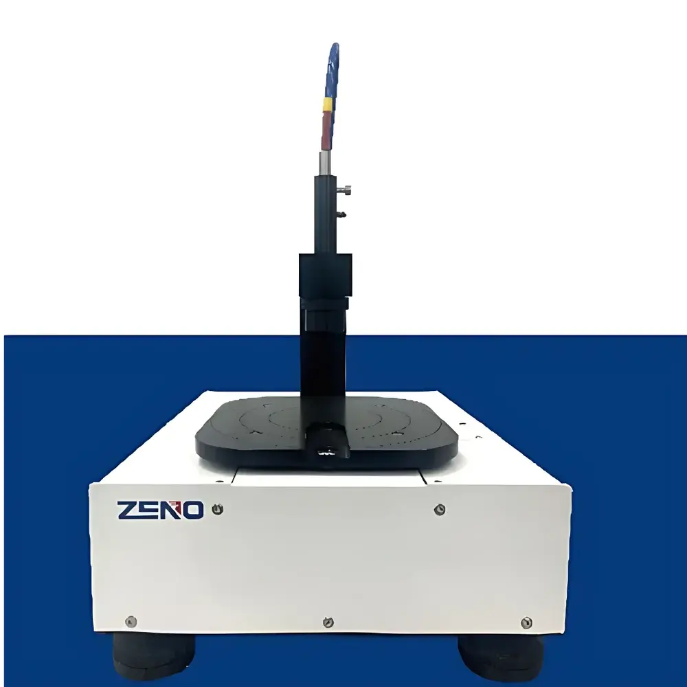
ZENO R100 Reflective Spectroscopic Ellipsometry & Thin-Film Metrology System
| Brand | ZENO |
|---|---|
| Model | R100 |
| Origin | Shanghai, China |
| Type | Benchtop Spectral Reflectometer |
| Measurement Principle | Broadband Spectral Reflectance Analysis (350–1000 nm) |
| Sample Compatibility | 4–8 inch wafers, square substrates, irregular shapes |
| Measurable Parameters | Film Thickness, Refractive Index (n), Extinction Coefficient (k), Reflectance (R) |
| Repeatability | ≤±0.15 nm (for 500 nm SiO₂ on Si, n=30) |
| Optical Spot Size | Standard 2 mm Ø |
| Software | ZENO-Metro v4.x with GLP-compliant audit trail, data export (CSV, XML), and ASTM E2372-22 compliant reporting |
| Compliance | ISO/IEC 17025-ready workflow architecture, supports FDA 21 CFR Part 11 electronic signature configuration |
Overview
The ZENO R100 is a compact, benchtop spectral reflectometer engineered for non-contact, non-destructive metrology of single-layer and multi-layer thin films in semiconductor process development and front-end manufacturing environments. It operates on the physical principle of broadband spectral reflectance analysis—measuring intensity-based interference patterns across the visible to near-infrared spectrum (350–1000 nm)—to extract film thickness, complex refractive index (n + ik), and surface reflectance with high reproducibility. Unlike traditional ellipsometers requiring precise angular alignment and polarization optics, the R100 leverages fixed-angle, multi-wavelength reflectance modeling to deliver rapid, robust measurements without manual optical recalibration. Its design targets routine QC/QA tasks in fab environments where speed, stability, and operator independence are critical—particularly for monitoring dielectric stacks (SiO₂, Si₃N₄), semiconductor layers (poly-Si, a-Si), photoresists, transparent conductive oxides (ITO, AZO), and polymer films (PI, BCB) on silicon, glass, or sapphire substrates.
Key Features
- Broadband spectral measurement engine covering 350–1000 nm with 1 nm spectral resolution and thermoelectrically stabilized CCD detector
- Simultaneous extraction of thickness, refractive index (n), extinction coefficient (k), and absolute reflectance (R) from a single acquisition
- Fixed 6° or 12° incidence geometry optimized for high signal-to-noise ratio on planar and moderately curved surfaces
- Modular optical head compatible with optional micro-spot configuration (<100 µm diameter) for localized analysis of patterned wafers or edge characterization
- Integrated motorized XYZ stage (optional) enabling automated mapping across 8-inch wafers with sub-micron positional repeatability
- Real-time model fitting using Levenberg-Marquardt algorithm with built-in library of >200 dispersion models (Cauchy, Sellmeier, Tauc-Lorentz, Cody-Lorentz)
Sample Compatibility & Compliance
The R100 accommodates rigid planar substrates up to 200 mm (8 inch) in diameter, including standard silicon wafers, quartz blanks, fused silica masks, and ceramic carriers. Non-circular samples—such as square SOI wafers, diced dies, or custom-shaped photomask blanks—are supported via user-defined coordinate referencing within the software. All measurement protocols adhere to foundational thin-film metrology standards, including ASTM E2372-22 (Standard Practice for Spectroscopic Reflectance Measurements of Thin Films) and ISO 9277 (Surface chemical analysis — X-ray photoelectron spectroscopy — Calibration of binding energy scale). The system’s firmware and software architecture support GLP/GMP-aligned workflows, with full audit trail logging, user access control tiers, and optional 21 CFR Part 11 compliance modules for regulated semiconductor fabs and packaging facilities.
Software & Data Management
ZENO-Metro v4.x provides an intuitive, task-oriented interface designed for both novice operators and metrology engineers. Core capabilities include real-time spectral preview, multi-layer stack modeling with constraint propagation, batch recipe management, and automated pass/fail thresholding against process specifications. Data is stored in a relational SQLite database with timestamped metadata (operator ID, instrument serial, environmental conditions), supporting traceability per ISO/IEC 17025 requirements. Export formats include CSV (for SPC integration), XML (for MES connectivity), and PDF reports with embedded spectra, fit residuals, and uncertainty estimates. Remote diagnostics and firmware updates are performed over secure TLS-encrypted HTTP, with configurable backup to network drives or cloud storage endpoints.
Applications
- Process monitoring of gate oxide, interlayer dielectrics (ILD), and hard mask layers during CMOS fabrication
- Photoresist thickness uniformity mapping pre- and post-bake for lithography process control
- Characterization of transparent conductive films (ITO, FTO) in display and power device manufacturing
- Quality verification of anti-reflective coatings (ARC) and passivation layers on solar cells
- R&D validation of ALD/CVD-deposited nanolaminates and graded-index films
- Failure analysis of delamination or interfacial oxidation via k-value deviation tracking
FAQ
What is the minimum measurable thickness for amorphous silicon films?
For a-Si on SiO₂/Si substrates, the practical lower limit is ~2 nm, constrained by signal contrast and substrate roughness; accuracy improves significantly above 5 nm.
Can the R100 measure films on rough or textured surfaces?
Yes—within limits. Surface RMS roughness below 1 nm enables reliable modeling; for rougher surfaces (>2 nm RMS), effective medium approximation (EMA) models are available in software.
Is calibration required before each measurement session?
No. The system uses factory-characterized spectral response and drift-compensated reference measurements; only annual verification against NIST-traceable SiO₂/Si standards is recommended.
Does the software support custom scripting or API integration?
Yes. ZENO-Metro includes a documented COM interface and Python-compatible DLLs for integration into automated test sequences and factory automation systems (SECS/GEM, PyModbus).
How is measurement uncertainty quantified and reported?
Uncertainty is calculated per GUM (JCGM 100:2018) using Monte Carlo propagation across spectral noise, model parameter correlation, and reference standard uncertainty—reported alongside each measurement result.
Related Products


