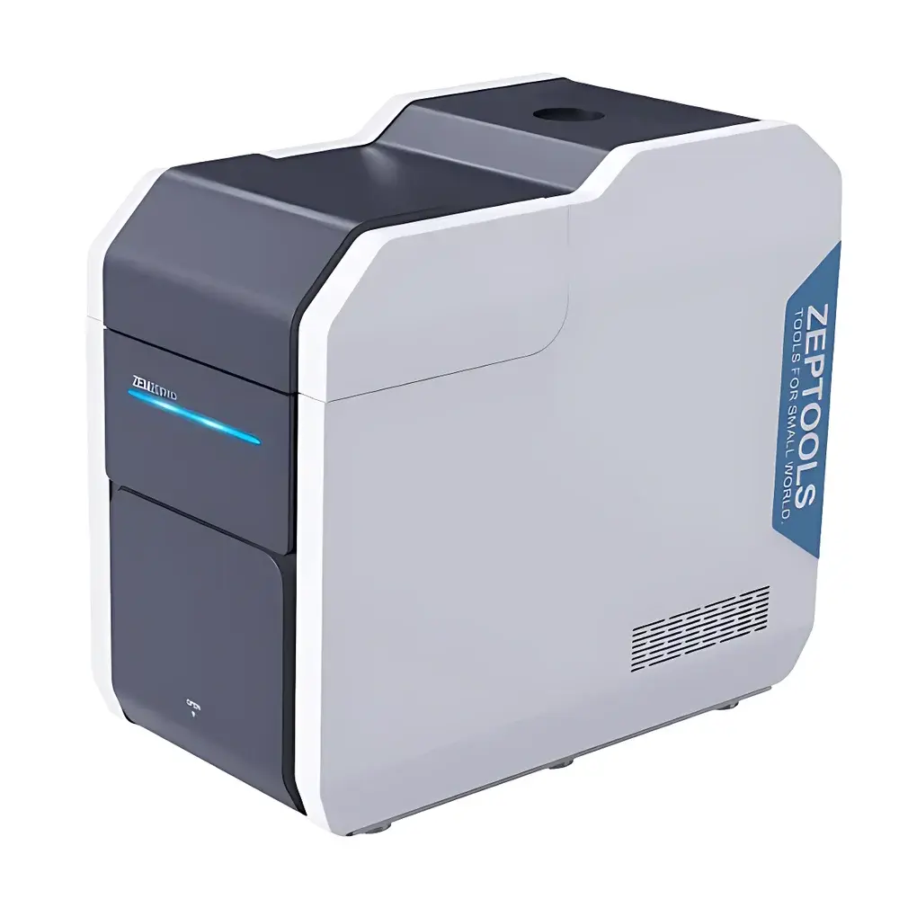
ZEPTOOLS Custom-Integrated Alloy Fabrication and In-Situ Compositional Analysis Platform with SEM-EDS
| Brand | ZEPTOOLS |
|---|---|
| Origin | Anhui, China |
| Manufacturer Type | Direct Manufacturer |
| Product Origin | Domestic (China) |
| Model | Custom-Integrated SEM-EDS Platform |
| Price Range | USD 17,000 – 25,500 |
| Magnification Range | 10× – 360,000× (continuously adjustable, user-definable setpoints) |
| Best Imaging Resolution | 3 nm (at 30 kV, SE mode) |
| EDS Detector | Silicon Drift Detector (SDD), ≥10 eV energy resolution (Mn-Kα) |
| Stage Dimensions | 540 mm × 760 mm |
| Motion Axes | 4-axis (X, Y, U, V) motorized precision stage |
| Minimum Positioning Increment | 0.001 mm |
| EDS Quantification Accuracy | ±2–5 wt% (matrix-dependent, per ISO 16529:2014 and ASTM E1508) |
Overview
The ZEPTOOLS Custom-Integrated Alloy Fabrication and In-Situ Compositional Analysis Platform is a purpose-built, modular scientific infrastructure system combining high-resolution scanning electron microscopy (SEM) with energy-dispersive X-ray spectroscopy (EDS) and synchronized precision mechanical alloy processing capabilities. Engineered for materials science laboratories engaged in advanced metallic alloy development, this platform enables real-time correlation between microstructural evolution—observed at sub-3 nm resolution—and localized chemical composition—quantified via calibrated EDS mapping and point analysis. Unlike conventional standalone SEMs or post-fabrication analytical workflows, the system integrates a large-format 4-axis motorized stage (540 × 760 mm) directly into the vacuum-compatible chamber environment, allowing in-chamber sample manipulation, multi-zone thermal pre-treatment (optional integration), and sequential fabrication–imaging–analysis cycles without air exposure. The imaging principle relies on raster-scanned primary electron beam interaction with solid specimens, generating secondary electrons (SE), backscattered electrons (BSE), and characteristic X-rays; the latter are collected and spectrally resolved by a high-count-rate silicon drift detector (SDD) to yield spatially registered elemental distribution data.
Key Features
- Sub-3 nm resolution imaging at 30 kV in secondary electron (SE) mode, validated per ISO 16700:2016 Annex B calibration protocols
- Continuously adjustable magnification from 10× to 360,000×, supporting both wide-field survey imaging and atomic-scale grain boundary inspection
- Integrated 4-axis (X/Y/U/V) motorized stage with 0.001 mm minimum incremental positioning—enabling precise navigation across heterogeneous alloy samples up to 500 mm in diameter
- Dedicated EDS hardware suite featuring liquid-nitrogen-free SDD detection, 130+ eV Mn-Kα energy resolution, and real-time spectrum acquisition at >100,000 cps
- On-board quantification engine compliant with ZAF and φ(ρz) matrix correction models, traceable to NIST SRM reference materials (e.g., NIST 610, 612)
- Vacuum architecture optimized for dual-mode operation: high-vacuum SEM imaging (≤1 × 10⁻⁴ Pa) and low-vacuum EDS acquisition (≤10 Pa) to accommodate conductive and semi-conductive alloy substrates
Sample Compatibility & Compliance
The platform accommodates bulk metallic alloys—including Al-, Ti-, Ni-, Fe-, and Co-based systems—as well as additively manufactured (AM) builds, diffusion-bonded laminates, and gradient composition specimens. Sample height tolerance extends to 120 mm under standard chamber configuration. All EDS quantitative outputs adhere to ISO 16529:2014 (Microanalysis — Quantitative analysis by energy-dispersive X-ray spectrometry) and ASTM E1508-19 (Standard Guide for Quantitative Analysis by Energy-Dispersive Spectroscopy). System design meets CE marking requirements under the EU Machinery Directive 2006/42/EC and Electromagnetic Compatibility Directive 2014/30/EU. Optional GLP-compliant audit trail logging supports FDA 21 CFR Part 11 readiness when paired with validated software modules.
Software & Data Management
Control and analysis are executed via ZEPTOOLS’ proprietary SEM-EDS Suite v4.2—a Windows 10/11–based application certified for ISO/IEC 17025:2017 laboratory informatics compliance. Core functionalities include automated drift compensation, multi-region EDS map stitching (up to 100 tiles), phase identification using integrated Thermo-Calc™ thermodynamic database linkage, and export of ASTM E1359–compliant compositional reports. Raw image and spectrum datasets are stored in vendor-neutral formats (TIFF, .emsa, .msa) with embedded metadata (acquisition voltage, working distance, dwell time, detector geometry). Audit logs record all user actions, parameter changes, and calibration events with timestamped digital signatures.
Applications
- In-process characterization of laser powder bed fusion (LPBF) and directed energy deposition (DED) alloy builds, including porosity tracking and intermetallic phase segregation analysis
- Interfacial reaction zone quantification in dissimilar metal welds (e.g., stainless steel–Inconel® joints) under thermal cycling conditions
- Grain boundary chemistry mapping in creep-resistant superalloys to correlate Cr/Mo depletion with oxidation resistance degradation
- High-throughput screening of combinatorial alloy libraries fabricated via sputter-deposited thin-film gradients
- Failure analysis of turbine blade coatings, focusing on TGO (thermally grown oxide) thickness and elemental interdiffusion profiles
FAQ
Is this system compatible with third-party EDS detectors or software?
Yes—hardware interfaces conform to the EDAX/Thermo Fisher EDS communication protocol standard (EDAX EDS API v3.1), enabling integration with legacy SDD detectors and optional import of spectra into commercial platforms such as Oxford Instruments AZtec or Bruker ESPRIT.
What vacuum pumping configuration is used?
A two-stage system comprising a turbomolecular pump (≥600 L/s for N₂) backed by a dry scroll pump ensures rapid pump-down (<15 min to operating pressure) and stable base vacuum during extended mapping sessions.
Can the platform perform automated particle analysis on inclusion populations?
Yes—the included Particle Analysis Module complies with ASTM E1245-21 and ISO 9276-2:2019, supporting size, shape, and compositional classification of non-metallic inclusions in steels and aluminum alloys.
Is remote operation supported for multi-user lab environments?
Remote desktop access is enabled via TLS-encrypted VNC with role-based permissions (operator, analyst, administrator); full session recording is available for internal QA review.
What maintenance intervals are recommended for optimal EDS performance?
Detector window integrity and spectral calibration verification are scheduled every 250 operational hours; annual full-system alignment and vacuum integrity testing are advised per ZEPTOOLS Service Bulletin SEM-EDS-2024-01.


