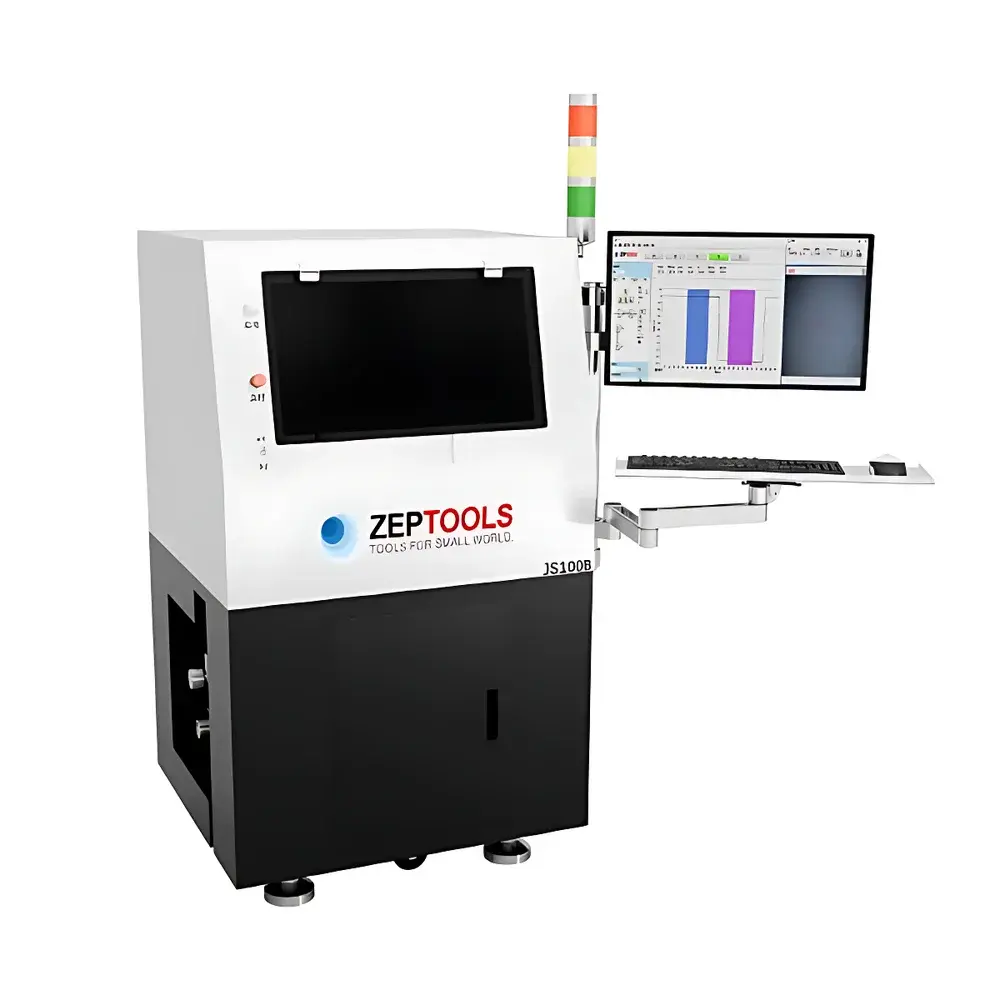
ZEPTOOLS JS100C Precision Step Height Measurement System
| Brand | ZEPTOOLS |
|---|---|
| Origin | Guangdong, China |
| Manufacturer Type | Original Equipment Manufacturer (OEM) |
| Product Category | Domestic |
| Model | JS100C |
| Pricing | Available upon Request |
| Measurement Principle | Inductive (LVDT-based) |
| Vertical Measurement Range | 160 µm |
| Probe Tip Radius | 2 µm / 1 µm (interchangeable) |
| Probe Normal Force | 0.5–50 mg |
| Scan Length | 55 mm |
| Step Height Repeatability | < 0.5 nm |
| Vertical Resolution | 0.05 nm (full-scale) |
| Maximum Sample Size | 150 mm × 150 mm |
Overview
The ZEPTOOLS JS100C is a semi-automated, high-precision step height measurement system engineered for nanoscale topographic characterization in semiconductor process development and thin-film metrology. Based on inductive displacement sensing—specifically linear variable differential transformer (LVDT) technology—the instrument delivers sub-nanometer vertical resolution and exceptional thermal and mechanical stability. Its monolithic granite base structure minimizes vibration coupling and thermal drift, enabling repeatable measurements under standard laboratory conditions without active environmental control. Designed to meet the stringent requirements of front-end semiconductor fabrication, the JS100C supports traceable, non-destructive profilometry of patterned wafers, etched features, deposited films, and MEMS structures. It serves as a critical tool for process validation, yield analysis, and quality assurance across R&D, pilot-line, and production environments.
Key Features
- Monolithic granite frame with precision-ground granite stage for long-term dimensional stability and low thermal expansion coefficient (< 2 µm/m·°C).
- Dual high-resolution color cameras (coaxial + oblique view) providing real-time, distortion-free imaging of both probe tip and sample surface—enabling precise feature targeting and automated scan alignment.
- Interchangeable probe tips with radii of 1 µm and 2 µm, optimized for high-resolution profiling of steep sidewalls or ultra-smooth surfaces respectively.
- Programmable probe normal force (0.5–50 mg) with closed-loop feedback control, ensuring consistent contact pressure across diverse film hardnesses and substrate types.
- Motorized X-Y-Z positioning system with 55 mm linear scan range and sub-micron repeatability, supporting both single-line and multi-point raster scanning.
- Integrated 3D surface reconstruction engine capable of generating ISO-compliant areal surface texture parameters (Sa, Sq, Sz, etc.) and cross-sectional profiles compliant with ISO 25178 and ISO 4287 standards.
Sample Compatibility & Compliance
The JS100C accommodates flat, rigid substrates up to 150 mm × 150 mm (standard configuration), with optional stages available for 200 mm and 300 mm wafers. It is compatible with silicon, sapphire, quartz, glass, metal, and polymer substrates—provided surface roughness (Ra) remains below 5 nm to ensure reliable tip tracking. The system meets mechanical safety requirements per IEC 61000-6-2 (immunity) and IEC 61000-6-3 (emissions). All measurement data output conforms to ASTM E2921-22 (Standard Guide for Profilometric Measurements of Thin-Film Thickness) and supports traceability via NIST-traceable calibration artifacts. Audit trails, user access logs, and electronic signatures are configurable to align with GLP and GMP documentation practices.
Software & Data Management
The proprietary ZEPTOOLS ProfilSoft™ v4.2 software provides intuitive workflow-driven operation—from sample setup and feature selection to automated measurement execution and statistical reporting. It supports batch processing of multi-site scans, customizable report templates (PDF/CSV/XLSX), and direct export of height maps in common formats (STL, OBJ, XYZ). Raw profile data is stored in HDF5 format with embedded metadata (timestamp, operator ID, calibration status, environmental conditions). The software architecture complies with FDA 21 CFR Part 11 requirements when configured with role-based authentication, electronic signature enforcement, and immutable audit logging.
Applications
- Thickness metrology of PVD/CVD-deposited films (e.g., SiO₂, SiNₓ, TiN, Al, Cu) on patterned wafers.
- Etch depth uniformity assessment in gate-last and finFET processes—including 18 nm node test structures.
- Surface roughness and waviness quantification of polished wafers, optical coatings, and micro-optical components.
- Thin-film stress calculation via wafer curvature mapping using Stoney’s equation (requires optional full-wafer bow module).
- 3D morphology analysis of MEMS cantilevers, microfluidic channels, and photomask relief structures.
- Multi-point monitoring for process drift detection during plasma etch or ALD chamber qualification.
FAQ
What is the vertical resolution specification—and is it guaranteed over the full 160 µm range?
The system achieves 0.05 nm resolution at full scale, verified by interferometric calibration using NIST-traceable step standards; resolution remains constant across the entire measurement range due to digital LVDT signal conditioning.
Can the JS100C measure steps with slopes exceeding 70°?
Yes—using the 1 µm radius probe tip and adaptive force control, the system reliably tracks sidewalls up to 85°, provided surface reflectivity and cleanliness meet standard SEM-grade preparation criteria.
Is the software compatible with Windows 11 and 64-bit architectures?
Yes—ProfilSoft™ v4.2 is natively compiled for Windows 10/11 (64-bit) and supports DirectX 12-accelerated rendering for real-time 3D visualization.
Does the system support automated calibration routines?
Yes—integrated auto-calibration includes probe tip radius verification, force sensor zeroing, and stage linearity correction using built-in reference gratings and certified step standards.
How is data integrity ensured during long-duration multi-point campaigns?
Each measurement event is timestamped, digitally signed, and appended to an encrypted SQLite database with SHA-256 hash chaining—ensuring tamper-evident audit trails required for ISO 17025 accreditation.