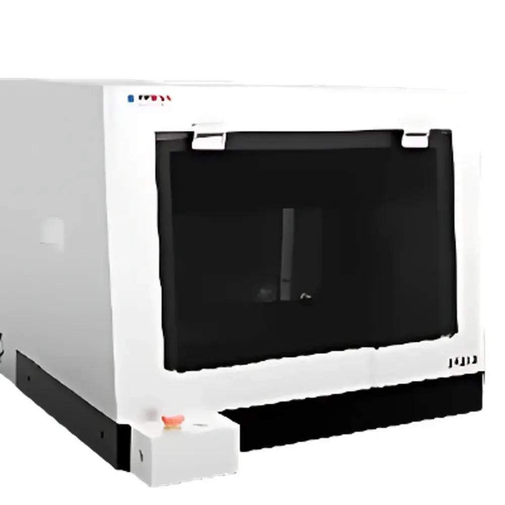
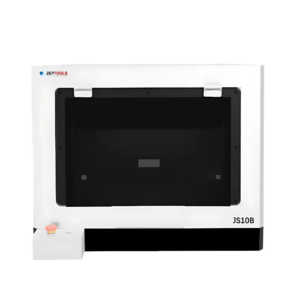
ZEPTOOLS JS10C Manual Stylus Profilometer
| Brand | ZEPTOOLS |
|---|---|
| Origin | Guangdong, China |
| Manufacturer Type | Direct Manufacturer |
| Model | JS10C |
| Measurement Principle | Inductive |
| Vertical Measurement Range | 160 µm |
| Probe Tip Radius | 2 µm / 1 µm (interchangeable) |
| Normal Force Range | 0.5–50 mg |
| Scan Length | 55 mm |
| Step Height Repeatability | < 0.5 nm |
| Vertical Resolution | 0.05 nm (full-scale) |
| Maximum Sample Size | 150 mm (Ø) |
| Scan Resolution | 10 nm |
| Scan Speed | 5–1000 µm/s |
| Max Data Points per Scan | 2,000,000 |
| Software Functions | Step Height, Surface Roughness (Ra, Rq, Rz, etc.), Flatness, Warp Measurement |
Overview
The ZEPTOOLS JS10C Manual Stylus Profilometer is a high-precision, benchtop surface topography measurement system engineered for quantitative micro- and nanoscale step height, roughness, flatness, and warp characterization. It operates on the principle of inductive displacement sensing—where a diamond-tipped stylus physically traverses the sample surface, and minute vertical deflections are transduced via a high-stability linear variable differential transformer (LVDT) sensor. This contact-based profilometry method delivers traceable, SI-referenced height data with exceptional signal-to-noise ratio and long-term thermal stability. The instrument features a monolithic granite base structure that minimizes vibration coupling and thermal drift, ensuring mechanical rigidity essential for sub-nanometer repeatability. Designed specifically for R&D labs and process control environments in semiconductor fabrication, MEMS development, thin-film coating evaluation, and advanced packaging, the JS10C supports rigorous metrology workflows without requiring active environmental isolation.
Key Features
- Monolithic granite frame with precision-machined granite stage for superior dimensional stability and vibration damping
- Interchangeable stylus tips (1 µm and 2 µm radius) enabling optimization for high-resolution step edges or low-force scanning of soft films
- Adjustable normal force control (0.5–50 mg) with real-time feedback, critical for compliant substrates such as photoresists, polymers, and low-k dielectrics
- Full-scale vertical resolution of 0.05 nm and step height repeatability better than 0.5 nm (verified using NIST-traceable step standards over 30 repeated scans)
- Integrated high-resolution color CCD camera with 10× optical zoom and live overlay crosshair for precise probe positioning and scan region verification
- Manual XYZ stage with fine micrometer controls (X/Y: 100 mm travel; Z: 50 mm lift), calibrated to ±0.5 µm accuracy
- Scan length up to 55 mm at selectable lateral resolutions down to 10 nm, supporting full-wafer mapping of 150 mm (6-inch) substrates
Sample Compatibility & Compliance
The JS10C accommodates rigid and semi-rigid planar samples up to Ø150 mm and 25 mm thick, including silicon wafers, glass substrates, ceramic carriers, metal foils, and polymer films. Its low-force scanning capability enables reliable profiling of delicate layers such as spin-on carbon hard masks, ALD-grown oxides, and electroplated copper interconnects without tip-induced deformation. All measurement protocols adhere to ISO 25178-2 (areal surface texture) and ISO 4287 (profile-based roughness), while step height analysis aligns with SEMI MF1529 and ASTM E1399 standards. Data integrity is maintained through GLP-compliant audit trails, user-access logging, and timestamped raw profile export in ASCII and CSV formats—fully compatible with external statistical process control (SPC) platforms.
Software & Data Management
The proprietary ZEPTOOLS Profilometer Suite v4.x provides intuitive workflow-driven operation with dual-mode interface: manual scan setup for rapid QA checks and scriptable batch acquisition for unattended multi-site measurements. Core modules include ISO-compliant roughness analysis (Ra, Rq, Rz, Rsk, Rku, Rmr), step height quantification with automatic edge detection and baseline fitting (least-squares, polynomial, spline), flatness deviation mapping (per ISO 1101), and global warp calculation (bow and site flatness). All results are exportable with metadata (operator ID, timestamp, calibration ID, environmental log) in PDF reports or structured XML/JSON for LIMS integration. The software supports FDA 21 CFR Part 11 compliance via optional electronic signature module, role-based access control, and immutable audit logs.
Applications
- Semiconductor process monitoring: film thickness uniformity, etch depth, CMP endpoint verification, and lithographic resist profile metrology (e.g., 18 nm node gate structures)
- MEMS/NEMS device characterization: cantilever height, comb-drive gap uniformity, and release etch undercut quantification
- Advanced packaging: redistribution layer (RDL) step coverage, under-bump metallization (UBM) topography, and TSV sidewall inspection
- Optical component manufacturing: anti-reflective coating step transitions, diffractive optical element (DOE) groove depth, and micro-lens array form error
- Materials science: thin-film adhesion failure assessment, scratch resistance testing, and phase-separation morphology in block copolymers
FAQ
What calibration standards are recommended for routine verification of the JS10C?
NIST-traceable step height standards (e.g., VLSI Standards SRM 2130 series) with certified values between 10 nm and 100 µm are recommended for daily system performance checks. ZEPTOOLS provides a certified 100 nm and 1 µm reference standard with each instrument.
Can the JS10C measure non-conductive or insulating samples?
Yes—the inductive sensing mechanism is independent of sample conductivity. No conductive coating or charge dissipation is required, making it suitable for SiO₂, Si₃N₄, photoresists, and polyimide films.
Is automated multi-point mapping supported?
The JS10C is manually operated; however, its software supports pre-defined coordinate lists for operator-guided sequential scanning across up to 99 locations, with auto-save and batch report generation.
How is thermal drift compensated during extended scans?
The granite base exhibits coefficient of thermal expansion (CTE) < 1 µm/m·°C. Combined with internal temperature monitoring and zero-drift correction algorithms applied during post-processing, thermal effects are reduced to < 0.1 nm/°C over typical lab conditions (20–25 °C).
Does the system support third-party data analysis tools?
Raw profile data is exported in ASCII format with header metadata, fully compatible with MATLAB, Python (NumPy/Pandas), MountainsMap, and Gwyddion for advanced spectral or fractal analysis.