ZEPTOOLS SEM Nano-Probe Station
| Brand | ZEPTOOLS |
|---|---|
| Origin | Guangdong, China |
| Manufacturer Type | OEM Manufacturer |
| Product Category | Domestic |
| Model | SEM Nano-Probe Station |
| Pricing | Upon Request |
| XYZ Travel Range | ±10 mm |
| Fine-Adjustment Resolution | 0.5 nm |
| Sample Stage Flatness | 10 µm |
| Total Probe Station Mass | 225 g |
| Max. Translation Speed | 3 mm/s |
| Motion Guidance | Zero-Gap Flexure Hinge System |
| Actuation | Piezoelectric Ceramic Positioning Stages |
| Optional Modules | Cryogenic Stage, High-Temperature Stage, Fiber Optic Feedthrough & Clamp, EBIC Kit |
Overview
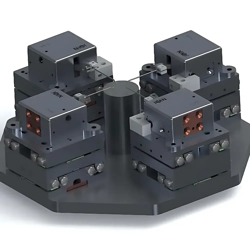
The ZEPTOOLS SEM Nano-Probe Station is an ultra-compact, high-rigidity in-chamber nanomanipulation platform engineered for integration within scanning electron microscope (SEM) and focused ion beam (FIB) vacuum chambers. It operates on a three-axis orthogonal piezoelectric actuation architecture—comprising independent X, Y, and Z motion stages—enabling sub-nanometer positional control inside the high-vacuum environment of modern analytical electron microscopes. Unlike conventional motorized or stepper-based probe systems, this station employs zero-backlash flexure hinge guidance to eliminate mechanical play and hysteresis, ensuring repeatable positioning accuracy critical for in situ nanoscale electrical, optical, and mechanical characterization. Its modular design permits simultaneous installation of multiple units within a single SEM chamber, supporting parallel multi-probe experiments such as four-point probe resistivity mapping, current–voltage (I–V) spectroscopy, electron-beam-induced current (EBIC) imaging, and nanomechanical force probing.
Key Features
- Ultra-low mass construction (225 g total) minimizes thermal drift and vibration coupling during high-magnification imaging.
- Flexure-guided XYZ stages with 0.5 nm fine-resolution adjustment, calibrated via integrated capacitive or strain-gauge position feedback (optional).
- Vacuum-compatible feedthroughs rated for ≤1×10⁻⁷ mbar; includes standardized CF or KF flange interfaces for seamless integration with JEOL, Hitachi, Thermo Fisher (FEI), and TESCAN SEM/FIB systems.
- Modular probe head interface accepts industry-standard holders for electrical probes (tungsten, Pt/Ir), optical fibers (single-mode or multimode), diamond nanoindenter tips, microinjection pipettes, and nanotweezers.
- Piezoceramic actuators rated for >10¹⁰ cycles under continuous operation—ensuring long-term stability without lubrication or wear-related recalibration.
Sample Compatibility & Compliance
The station supports planar and tilted sample geometries up to 10 µm surface flatness tolerance, compatible with standard SEM stubs (12.7 mm, 25 mm, or custom-diameter mounts). All structural components are fabricated from non-magnetic, ultra-high vacuum (UHV)-compatible alloys (e.g., titanium alloy Ti-6Al-4V and oxygen-free copper), minimizing outgassing and secondary electron interference. The system complies with ISO 14644-1 Class 5 cleanroom handling protocols during assembly and meets ASTM E1558 guidelines for in situ nanomanipulation instrumentation. Optional cryogenic (4 K–300 K) and high-temperature (up to 800 °C) sample stages are available with integrated temperature sensors and PID controllers, enabling thermally dependent property mapping under SEM observation.
Software & Data Management
Control is executed via a dedicated USB-connected probe controller with analog/digital I/O ports for synchronized acquisition with external source-measure units (SMUs), lock-in amplifiers, or spectrometers. The accompanying ZEPTOOLS Control Suite provides scriptable motion sequencing (Python API), real-time coordinate logging, and time-stamped metadata tagging compliant with GLP/GMP audit requirements. Data export formats include CSV, HDF5, and MDA (for compatibility with Gatan DigitalMicrograph and Thermo Scientific Avizo). Optional FDA 21 CFR Part 11-compliant electronic signature modules support regulated semiconductor R&D environments requiring traceable operator actions and instrument calibration history.
Applications
- In situ electrical transport measurements of 2D materials (graphene, TMDCs), nanowires, and quantum dot devices.
- EBIC and cathodoluminescence (CL) correlation studies for defect localization in III–V heterostructures and SiC power devices.
- Mechanical property extraction via nanoindentation-assisted stress–strain mapping inside FIB-SEM dual-beam systems.
- Single-cell manipulation and intracellular injection under real-time SEM imaging—validated for fixed and freeze-dried biological specimens.
- Integration with AFM-SEM hybrid platforms for correlative topographical–electrical–mechanical analysis.
FAQ
Is the probe station compatible with field-emission SEMs operating at 1 kV or lower accelerating voltage?
Yes—the low-outgassing materials and minimal secondary electron yield of the Ti-6Al-4V structure ensure stable operation even under low-kV conditions without charging artifacts.
Can the system be retrofitted into an existing SEM chamber without chamber venting?
Installation requires chamber venting only once; subsequent probe swaps or module additions (e.g., fiber feedthroughs) are performed through auxiliary ports without breaking main vacuum.
What level of positional reproducibility is achievable over 24-hour continuous operation?
Under constant thermal conditions (±0.5 °C), positional drift remains below ±2 nm RMS over 24 h—verified per ISO 230-2 Annex B test protocols.
Does ZEPTOOLS provide application-specific calibration certificates?
Yes—NIST-traceable calibration reports for displacement linearity, orthogonality, and resolution are issued per unit upon request, aligned with ISO/IEC 17025 laboratory accreditation standards.


