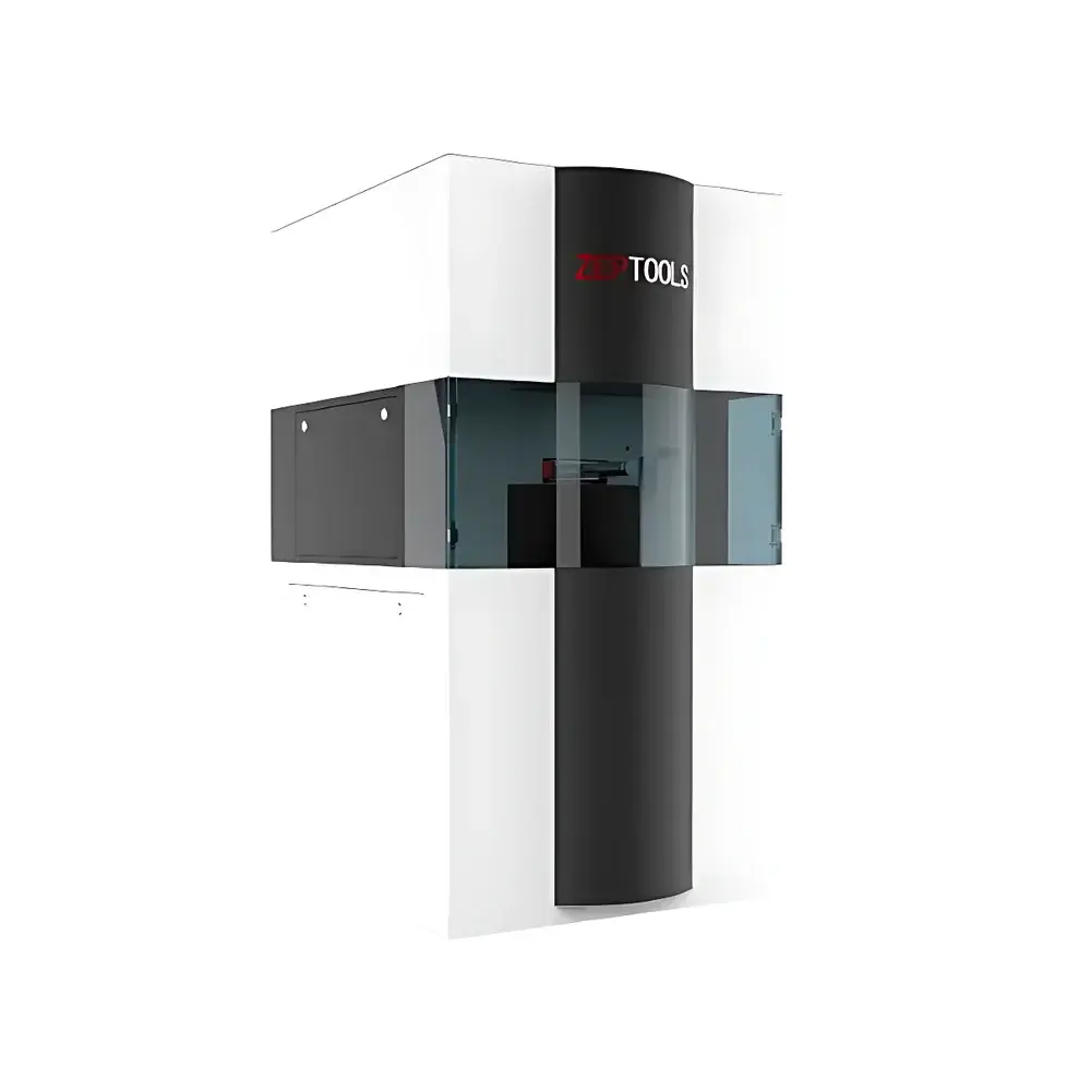
ZEPTOOLS ZEL304G Electron Beam Lithography System
| Brand | ZEPTOOLS |
|---|---|
| Origin | Guangdong, China |
| Manufacturer Type | Original Equipment Manufacturer (OEM) |
| Country of Origin | China |
| Model | ZEL304G |
| Pricing | Available upon request |
| Electron Source | Schottky field-emission gun |
| Acceleration Voltage | 20 V–30 kV |
| Image Resolution | ≤1 nm @ 15 kV, ≤1.5 nm @ 1 kV |
| Minimum Beam Spot Size | ≤2 nm |
| Beam Current | ≥100 nA |
| Beam Current Density | >7000 A/cm² |
| Beam Blanking Rise Time | <100 ns |
| Writing Field | ≥500 × 500 µm |
| Minimum Single-Exposure Line Width | <15 nm |
| Stage Travel | ≥105 mm |
| Stitching Accuracy | <50 nm (mean + 1σ) |
| Overlay Accuracy | <50 nm (mean + 1σ) |
| Scan Rate | ≥20 MHz (standard), up to 50 MHz (max) |
| D/A Resolution | 20-bit |
| Dwell Time Increment | 10 ns |
| Supported File Formats | GDSII, DXF, BMP |
| Scan Modes | Raster (Z-scan), serpentine (S-scan), spiral vector scanning |
| Exposure Modes | Field calibration, field stitching, multi-layer overlay, auto-exposure sequencing |
| Optional Features | Proximity effect correction (PEC), laser interferometric stage, Faraday cup beam current monitor, TTL-compatible beam blanking (5 V), external I/O for synchronized stage motion, beam blanking, SE detection, and scan control |
Overview
The ZEPTOOLS ZEL304G Electron Beam Lithography (EBL) System is a high-precision, research-grade direct-write nanofabrication platform engineered for advanced semiconductor process development, quantum device prototyping, photonic integrated circuit (PIC) fabrication, and fundamental condensed matter physics studies. Operating on the principle of focused electron beam scanning in vacuum, the ZEL304G utilizes a thermally assisted Schottky field-emission electron source to generate a stable, high-brightness beam with sub-2 nm minimum probe size. Combined with a high-bandwidth vector scanning architecture and real-time beam positioning feedback, the system delivers deterministic patterning at the <15 nm line-width scale—subject to resist process optimization and environmental stability. Its design prioritizes metrological traceability, mechanical robustness, and integration readiness within cleanroom environments compliant with ISO Class 5 (Class 100) standards.
Key Features
- High-stability Schottky field-emission electron gun with acceleration voltage range from 20 V to 30 kV, enabling flexible landing energy selection for resist sensitivity tuning and reduced substrate charging.
- Laser interferometer-based precision sample stage with ≥105 mm travel and closed-loop position feedback, delivering stitching and overlay accuracy better than 50 nm (mean + 1σ) across multi-field exposures.
- Ultra-high-speed FPGA-driven pattern generator supporting 50 MHz maximum scan rate, 10 ns dwell time resolution, and 20-bit digital-to-analog conversion for sub-pixel beam placement fidelity.
- Multi-mode scanning engine offering raster (Z-type), serpentine (S-type), and spiral vector trajectories—optimized for throughput, dose uniformity, and proximity effect mitigation.
- Integrated Faraday cup for in situ beam current monitoring and automatic dose calibration, ensuring reproducible exposure dosage across wafer batches and tool uptime.
- Modular I/O interface supporting synchronous coordination between beam blanking (TTL 5 V), stage motion, secondary electron (SE) signal acquisition, and external process triggers (e.g., resist development start).
Sample Compatibility & Compliance
The ZEL304G accommodates standard semiconductor substrates including Si, SiO₂/Si, SOI, GaAs, InP, sapphire, and quartz wafers up to 200 mm diameter (with optional chuck upgrade). It supports both positive and negative tone e-beam resists (e.g., PMMA, ZEP, HSQ, AR-P 6200) and is compatible with conventional spin-coating, hotplate soft-bake, and developer dispensing modules via third-party integration. The system meets electromagnetic compatibility (EMC) requirements per CISPR 11 Group 1, Class B, and incorporates active vibration isolation (natural frequency ≤2 Hz) and uninterruptible power supply (UPS) interfaces to maintain operational continuity during grid fluctuations. While not certified to ISO 9001 or FDA 21 CFR Part 11 out-of-the-box, its architecture supports audit-ready data logging, user access control, and electronic signature implementation when deployed under GLP/GMP-aligned laboratory quality systems.
Software & Data Management
Control and patterning are managed through ZEPTOOLS’ proprietary EBL Suite, a Windows-based application built on modular C++ libraries with Python API support for custom automation. The software natively imports industry-standard layout formats—including GDSII, DXF, and bitmap (BMP)—and provides hierarchical decomposition, dose modulation mapping, and proximity effect correction (PEC) using variable-shaped beam (VSB) or Gaussian beam models. All exposure parameters, beam current logs, stage position timestamps, and error flags are stored in SQLite-backed project databases with SHA-256 hash integrity verification. Export options include CSV metadata reports and TIFF/SEM-style image exports of acquired secondary electron frames—facilitating cross-platform metrology correlation with CD-SEM or AFM tools.
Applications
- Prototyping of quantum dot arrays, superconducting qubit architectures, and topological insulator nanostructures requiring atomic-scale registration fidelity.
- Development of high-resolution photomasks for EUV and DUV stepper evaluation, particularly for non-planar or low-throughput mask layers.
- Fabrication of plasmonic metasurfaces, photonic crystal cavities, and nanophotonic waveguides where sub-20 nm feature periodicity and edge roughness <2 nm RMS are critical.
- Materials science investigations involving lithographically defined heterostructure interfaces, strain-engineered 2D material devices, and ion-irradiated defect patterning templates.
- Microelectromechanical systems (MEMS) and NEMS device fabrication where sidewall verticality and aspect ratio >10:1 must be preserved without lift-off limitations.
FAQ
What vacuum level does the ZEL304G require for stable operation?
The system operates at a base pressure of ≤5 × 10⁻⁷ Pa (5 × 10⁻⁹ mbar) in the column and ≤1 × 10⁻⁵ Pa in the chamber, maintained by a combination of turbomolecular and ion getter pumps.
Is the ZEL304G compatible with automated wafer handling?
Yes—via optional front-end interface module supporting SECS/GEM communication protocols and alignment with standard FOUP/SMIF load ports.
Can the system perform real-time dose modulation during writing?
Yes—through dynamic dose lookup tables (DLUTs) updated at ≤1 MHz, synchronized with beam position and dwell time control.
Does the ZEL304G support multi-pass exposure strategies for high-aspect-ratio resist profiles?
Yes—exposure sequences can be programmed with layer-specific dwell times, beam currents, and focus offsets, all logged with full timestamped audit trails.
What service and calibration support is available outside mainland China?
ZEPTOOLS maintains authorized service partners in Germany, Singapore, and the United States, providing remote diagnostics, on-site preventive maintenance, and NIST-traceable stage calibration using calibrated grating standards.
Related Products


