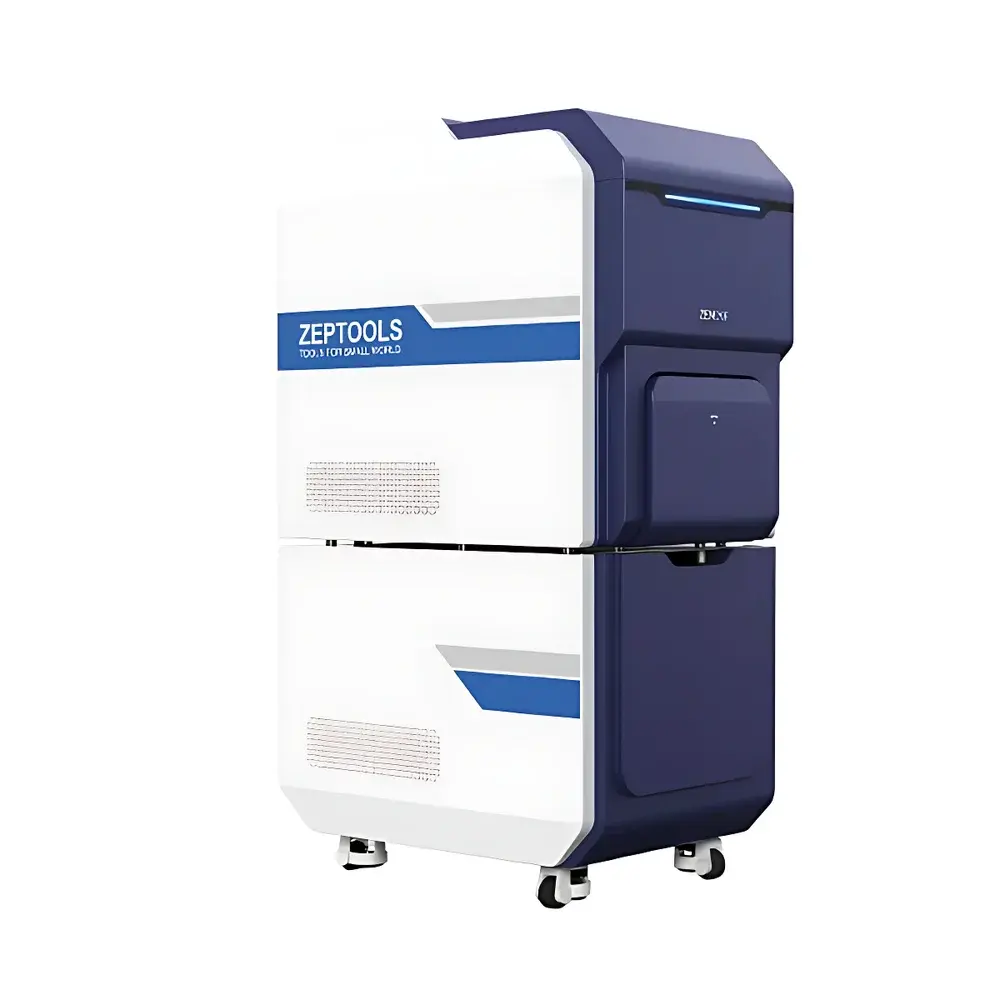
ZEPTOOLS ZEM Ultra Desktop Field Emission Scanning Electron Microscope
| Brand | ZEPTOOLS |
|---|---|
| Origin | Anhui, China |
| Manufacturer Type | Direct Manufacturer |
| Instrument Type | Desktop SEM |
| Electron Source | Schottky Field Emission Gun |
| Resolution (SE & BSE) | <2.5 nm |
| Max Magnification | 1,000,000× |
| Accelerating Voltage Range | 1–15 kV (continuously adjustable) |
| Stage | Motorized XY (optional XYZ/XYT/5-axis) |
| Detector Options | Secondary Electron (SE), Backscattered Electron (BSE), Energy-Dispersive X-ray Spectroscopy (EDS), Electron Backscatter Diffraction (EBSD) |
| Vacuum System | Triple-stage independent vacuum architecture |
| Imaging Modes | Standard SE/BSE, deceleration mode (0–10 kV sample bias, optional) |
| Image Acquisition | 512×512 (real-time video), 2048×2048 (high-res still capture) |
| Compliance | Designed for ISO/IEC 17025-aligned lab environments |
Overview
The ZEPTOOLS ZEM Ultra Desktop Field Emission Scanning Electron Microscope is an engineered solution for high-resolution microstructural characterization in compact laboratory spaces. Utilizing a thermally assisted Schottky field emission electron source, the system delivers stable, high-brightness electron beams with exceptional coherence and low energy spread—enabling sub-2.5 nm secondary and backscattered electron imaging resolution at accelerating voltages ranging from 1 kV to 15 kV. Its triple-stage independent vacuum architecture ensures rapid pump-down, long-term beam stability, and contamination resilience—critical for consistent imaging of beam-sensitive or non-conductive samples. Unlike conventional tungsten-filament desktop SEMs, the ZEM Ultra bridges the performance gap between benchtop accessibility and analytical-grade capability, making it suitable for routine quality control, materials R&D, and academic teaching labs where space, budget, and operational simplicity are constrained without compromising on fundamental imaging fidelity.
Key Features
- Schottky field emission electron gun with automatic alignment and lifetime monitoring—ensures >1,500 hours of continuous operation under standard conditions
- Motorized XY stage (with optional XYZ, XYT, or 5-axis configurations) for precise positional repeatability and multi-region navigation
- Large-chamber design accommodating specimens up to Ø100 mm × 50 mm height—compatible with standard SEM stubs, custom holders, and in situ stages
- Integrated dual-detector system: Everhart-Thornley SE detector and solid-state BSE detector for simultaneous topographic and compositional contrast acquisition
- Modular hardware expansion interface supporting EDS spectrometer integration (Si(Li) or SDD detectors) and EBSD pattern collection systems
- Deceleration mode (0–10 kV sample bias, optional) for low-voltage surface-sensitive imaging—reducing charging effects on insulating materials such as polymers, ceramics, and biological coatings
- Automated workflows including autofocus, auto-stigmation, and beam alignment—reducing operator dependency and training overhead
Sample Compatibility & Compliance
The ZEM Ultra accommodates a broad spectrum of conductive and non-conductive specimens—including metals, alloys, semiconductors, battery cathode/anode materials (e.g., LiFePO₄, SiO₂), nanomaterials (e.g., CNTs, Au nanoparticles), geological thin sections, and coated biological tissues. Conductivity enhancement via sputter-coating (Au/Pd or Cr) remains optional but not mandatory for many applications due to low-kV imaging capability. The instrument conforms to IEC 61000-6-3 (EMC emissions) and IEC 61000-6-2 (immunity) standards. Software logs meet GLP/GMP documentation requirements—including timestamped parameter records, user authentication, and audit-trail-enabled session history—supporting compliance with FDA 21 CFR Part 11 when paired with validated IT infrastructure.
Software & Data Management
Acquisition and analysis are managed through ZEPTOOLS’ proprietary SEM Suite v4.x—a Windows-based platform featuring real-time image stitching, particle analysis (size, shape, distribution), line profile extraction, and EDS spectral quantification (ZAF or φ(ρz) correction). All images and metadata (kV, WD, dwell time, magnification, detector gain, stage coordinates) are stored in TIFF + JSON sidecar format for traceability. Batch export supports ASTM E1558-compliant reporting templates. Remote access and multi-user role management (admin/operator/observer) are supported over LAN/WAN with TLS 1.2 encryption. Data integrity safeguards include automatic checksum validation and version-controlled firmware updates.
Applications
- Materials science: Grain boundary mapping in polycrystalline alloys, fracture surface analysis of composites, porosity quantification in sintered ceramics
- Battery research: Morphological evolution of cathode particles during cycling, SEI layer thickness estimation, lithium dendrite detection
- Nanotechnology: Diameter distribution analysis of carbon nanotubes, aggregation state assessment of colloidal nanoparticles
- Electronics: Cross-sectional inspection of solder joints, intermetallic compound identification, failure analysis of PCB traces
- Geosciences: Mineral phase discrimination via BSE contrast, pore-network modeling in shale reservoir analogues
- Life sciences: Freeze-fracture replica imaging of membrane structures, collagen fibril orientation in decalcified bone sections
FAQ
Is the ZEM Ultra compliant with ISO 14644-1 Class 5 cleanroom requirements for installation?
Yes—the instrument’s sealed column and oil-free vacuum pumps enable safe deployment in ISO Class 5 environments; full qualification support documentation is available upon request.
Can the system be upgraded to include EBSD functionality post-purchase?
Yes—hardware mounting points and electrical interfaces for EBSD detectors are pre-installed; only detector integration and software license activation are required.
What is the typical service interval for the Schottky emitter?
Under standard operating conditions (≤10 kV, ≤1 nA probe current), the emitter requires no routine replacement within 1,500 operational hours; automated diagnostics monitor emission current decay and signal stability.
Does the software support batch processing of multiple EDS maps?
Yes—SEM Suite includes scriptable batch mode for automated quantification across ≥100 EDS elemental maps, with customizable ROI definitions and statistical summarization per map layer.
Is remote troubleshooting supported via secure connection?
Yes—engineer-assisted diagnostics are enabled via encrypted VNC tunnel with configurable session timeout and two-factor authentication.


