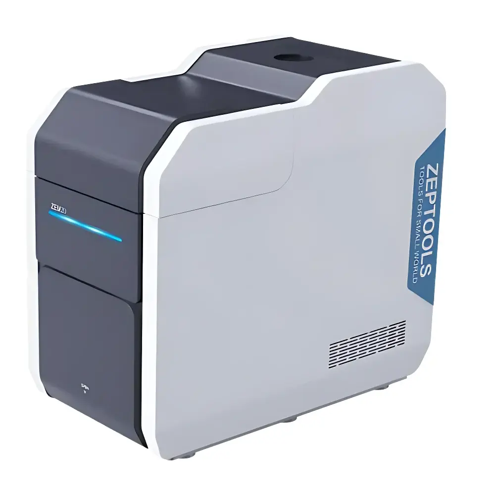
ZEPTOOLS ZEM20Pro Desktop Scanning Electron Microscope
| Brand | ZEPTOOLS |
|---|---|
| Origin | Anhui, China |
| Model | ZEM20Pro |
| Instrument Type | Desktop SEM |
| Electron Source | LaB₆ (Lanthanum Hexaboride) |
| Secondary Electron Resolution | 3 nm @ 30 kV |
| Backscattered Electron Resolution | 3 nm @ 30 kV |
| Magnification Range | 10× – 360,000× |
| Accelerating Voltage | 3–30 kV |
Overview
The ZEPTOOLS ZEM20Pro is a high-performance desktop scanning electron microscope (SEM) engineered for precision industrial metrology and failure diagnostics in regulated manufacturing environments. Operating on the principle of raster-scanned electron beam interaction with solid specimens, the ZEM20Pro generates high-fidelity secondary electron (SE) and backscattered electron (BSE) signals to resolve surface topography, phase contrast, and compositional variations at nanoscale resolution. Its LaB₆ thermionic electron source delivers stable beam current and superior signal-to-noise ratio compared to tungsten filaments—enabling consistent imaging across extended acquisition sessions without frequent filament replacement. Designed as a compact, benchtop-integrated system, the ZEM20Pro eliminates the need for dedicated high-bay laboratories or complex infrastructure while maintaining analytical rigor required for ISO/IEC 17025-compliant quality assurance workflows.
Key Features
- Sub-3 nm SE and BSE resolution at 30 kV—validated per ASTM E1558 for SEM performance characterization
- Wide accelerating voltage range (3–30 kV) supports low-voltage surface-sensitive imaging for beam-sensitive polymers, coatings, and biological composites, as well as high-penetration analysis of dense metals and ceramics
- Integrated motorized XYZ stage with ±90° tilt and 360° rotation enables multi-angle inspection of complex geometries—critical for turbine blade coatings, MEMS devices, and PCB interconnects
- Automated alignment routines—including auto-focus, auto-stigmation, and dynamic brightness/contrast optimization—reduce operator dependency and support unattended batch imaging
- Modular vacuum architecture with turbomolecular pumping achieves <1×10⁻³ Pa base pressure in <90 seconds, minimizing downtime between sample changes
- Optimized chamber geometry accommodates samples up to Ø100 mm × 50 mm height, supporting full wafers, machined components, and powder mounts without sectioning
Sample Compatibility & Compliance
The ZEM20Pro accommodates conductive and non-conductive industrial specimens via optional sputter coater integration (e.g., Au/Pd or Cr coating). For routine QC, standardized sample preparation protocols—including cryo-fracture, carbon tape mounting, and plasma cleaning—are documented in internal SOPs aligned with ISO 14644-1 cleanroom handling requirements. The system meets electromagnetic compatibility (EMC) standards per EN 61326-1 and electrical safety compliance per EN 61010-1. All imaging and measurement operations are traceable to NIST-traceable reference standards (e.g., NIST SRM 2461 Si grating), supporting GLP/GMP audit readiness and FDA 21 CFR Part 11–compliant data integrity frameworks when paired with validated software modules.
Software & Data Management
Acquisition and analysis are managed through ZEPTOOLS’ proprietary SEMControl Suite v4.2—a Windows-based platform featuring DICOM-compatible image export, calibrated pixel scaling, and embedded metrology tools compliant with ISO 16232 (for particle contamination analysis) and ISO 25178 (surface texture parameters). Measurement functions include line profile analysis, particle statistics (size, aspect ratio, circularity), grain boundary detection, and roughness parameter extraction (Sa, Sq, Sdr). Audit trail logging records user identity, timestamp, instrument settings, and calibration status for every acquired image—ensuring full data provenance. Raw image datasets (TIFF/RAW) and metadata are stored in hierarchical folder structures compatible with LIMS integration (e.g., Thermo Fisher SampleManager, LabWare).
Applications
- Quality Control: In-line verification of PCB trace width uniformity (±0.5 µm repeatability), solder joint morphology classification (IPC-A-610 Class 2/3), and ceramic capacitor electrode continuity
- Failure Analysis: Fractography of fatigue crack initiation sites in aerospace alloys; identification of intermetallic phases in Al-Si die-castings; mapping of chloride-induced pitting corrosion on stainless steel fasteners
- Process Optimization: Correlating thermal spray parameters (powder feed rate, standoff distance) with splat morphology and porosity distribution in TBCs; quantifying electroplated Ni layer thickness gradients via cross-sectional BSE imaging
- Raw Material Certification: Morphological screening of spherical Ti-6Al-4V powder (Dv50, sphericity, satellite count) per ASTM F3049; dispersion homogeneity assessment of carbon black in rubber compounds
- R&D Support: Interface characterization of CNT-reinforced polymer composites; dimensional validation of MEMS comb drives; nanostructure evolution during in-situ annealing of battery cathode materials
FAQ
Is the ZEM20Pro suitable for uncoated insulating samples?
Yes—low-kV imaging (≤5 kV) combined with charge compensation mode enables direct observation of ceramics, polymers, and glass without metallization in many cases. For quantitative EDS, however, conductive coating remains recommended.
What vacuum level is maintained during EDS acquisition?
The system sustains ≤5×10⁻⁴ Pa during simultaneous SEM-EDS operation, ensuring optimal X-ray detection efficiency and spectral peak resolution per ISO 14564.
Can measurement data be exported to statistical process control (SPC) platforms?
Yes—CSV exports include calibrated coordinates, measurement uncertainties, and operator metadata, enabling direct ingestion into Minitab, JMP, or custom Python-based SPC dashboards.
Does the system support automated image stitching for large-area metrology?
Yes—grid-based mosaic acquisition covers up to 10×10 mm fields with sub-pixel registration accuracy (≤0.3% geometric distortion), validated using NIST SRM 2462.
What is the mean time between failures (MTBF) for the LaB₆ source under typical industrial use?
Based on field data from >120 installed units, MTBF exceeds 1,800 hours at 20 kV/1 nA beam current—supported by predictive filament health monitoring in SEMControl Suite.


