ZEPTOOLS ZML10A Maskless Direct-Write Lithography System
| Brand | ZEPTOOLS |
|---|---|
| Origin | Guangdong, China |
| Manufacturer Type | Original Equipment Manufacturer (OEM) |
| Country of Origin | China |
| Model | ZML10A |
| Light Source | High-Intensity LED @ 405 nm |
| Uniformity | 96% |
| Minimum Achievable Feature Size | 0.5 µm |
| Exposure Field Size | 1.2 × 0.9 mm² (at 10× objective) |
Overview
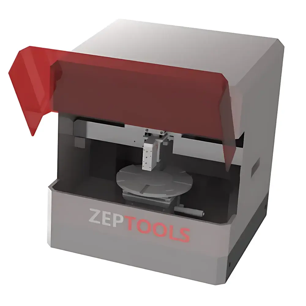
The ZEPTOOLS ZML10A Maskless Direct-Write Lithography System is a precision optical lithography platform engineered for research and pilot-scale microfabrication without the need for physical photomasks. It employs digital micromirror device (DMD)-based spatial light modulation combined with high-stability 405 nm LED illumination to project user-defined patterns directly onto photoresist-coated substrates via dynamic scanning exposure. This system operates on the principle of vector-scan or pixel-based pattern generation, enabling rapid prototyping of microstructures with sub-micron fidelity. Designed for cleanroom-compatible integration, the ZML10A supports wafer-level processing up to 4-inch diameter and is optimized for applications requiring iterative design cycles, low-volume fabrication, and process flexibility—particularly where mask cost, lead time, or design iteration frequency render conventional photolithography impractical.
Key Features
- Nanopositioning Stage with Piezo-Assisted Stitching: A high-resolution XYZ nanopositioning stage enables seamless field stitching across multiple exposure zones, maintaining overlay accuracy better than ±50 nm between adjacent fields.
- Real-Time Red-Light Alignment Guidance: Integrated 650 nm red LED alignment channel provides simultaneous visual feedback during pattern registration, supporting “what-you-see-is-what-you-write” alignment without interrupting UV exposure workflow.
- Optical Proximity Correction (OPC) Engine: Onboard pattern preprocessing applies model-based OPC algorithms to compensate for diffraction-induced line-end shortening, corner rounding, and linewidth bias—improving fidelity of dense and isolated features.
- Automated CCD-Based Focus Tracking: A coaxial CCD imaging module performs per-field autofocus by analyzing surface contrast in real time, ensuring consistent focal plane maintenance across non-planar or warped substrates.
- Uniform Illumination via Gray-Scale Homogenization: Custom-designed Köhler illumination optics coupled with dynamic intensity modulation deliver 96% irradiance uniformity across the full exposure field, minimizing dose variation and resist development non-uniformity.
Sample Compatibility & Compliance
The ZML10A accommodates standard silicon wafers (up to 100 mm), glass slides, quartz substrates, and flexible polymer films (e.g., PI, PET). Substrate thickness range: 0.1–2.0 mm. Chuck vacuum holding ensures flatness control within ±1.5 µm over 10 mm × 10 mm areas. The system complies with IEC 61000-6-3 (EMC emission standards) and IEC 61000-6-2 (immunity), and meets Class 1 laser safety requirements per IEC 60825-1 when operated with interlocked enclosure. While not certified for GMP manufacturing environments, its logging architecture supports GLP-aligned documentation practices—including timestamped exposure logs, parameter audit trails, and operator ID tagging—facilitating traceability in academic, government lab, and pre-commercial R&D settings.
Software & Data Management
Controlled via ZEPTOOLS LithoSuite™ v3.x, a Windows-based application supporting GDSII, OASIS, and SVG import. The software includes layer stacking, Boolean operations, hierarchical pattern editing, and real-time DMD bitplane simulation. All exposure parameters—including dose mapping, focus offset tables, and stitching offsets—are stored in XML-based project files with SHA-256 checksums for integrity verification. Export options include CSV-formatted exposure logs and PNG overlays for metrology correlation. Data export paths are configurable to network shares or local NAS, and optional audit trail modules support FDA 21 CFR Part 11–compliant electronic signatures and change history retention (requires licensed add-on).
Applications
- MEMS device prototyping: Fabrication of cantilevers, accelerometers, and microfluidic channels with feature sizes down to 500 nm.
- Photonic integrated circuit (PIC) test structures: Rapid iteration of grating couplers, waveguide bends, and ring resonators on SOI or SiN platforms.
- Lab-on-a-chip development: Patterning of electrode arrays, hydrophobic/hydrophilic boundary layers, and microchannel networks in PDMS and SU-8.
- LED and micro-LED substrate patterning: Definition of current-spreading layers, mesa isolation trenches, and reflective mirror patterns on sapphire or GaN wafers.
- Bio-MEMS and biosensor fabrication: Direct writing of antibody-binding regions, nanoimprint templates, and cell-adhesion topographies on functionalized surfaces.
FAQ
What substrates can be used with the ZML10A?
Standard substrates include silicon wafers (1–4 inch), fused silica, borosilicate glass, quartz, and polymer films such as polyimide and PET. Thickness must be between 0.1 mm and 2.0 mm.
Is the system compatible with standard positive and negative photoresists?
Yes—it supports common i-line resists (e.g., AZ® series, ma-N, SU-8) and is optimized for 405 nm sensitivity; resist selection should align with published quantum yield data at this wavelength.
Does the ZML10A support grayscale lithography?
Yes—via time-modulated DMD addressing, enabling controlled dose gradients for 3D microstructure fabrication (e.g., microlenses, diffractive optical elements).
Can exposure recipes be exported and shared between instruments?
All project files (.zlp) are portable across ZML10A units running identical firmware versions; calibration-specific parameters (e.g., focus map, stitching offsets) are stored separately and require site-specific validation.
What maintenance is required for long-term stability?
Recommended quarterly inspection of DMD cooling airflow, LED output power calibration using NIST-traceable photodiode, and stage encoder recalibration—documented in the Maintenance Log module of LithoSuite™.


