Zhengye XG Series Semiconductor X-ray Non-destructive Inspection System
| Brand | Zhengye |
|---|---|
| Origin | Guangdong, China |
| Manufacturer Type | OEM/ODM Manufacturer |
| Country of Origin | China |
| Model | XG Series |
| Price Range | USD 70,000 – 112,000 |
Overview
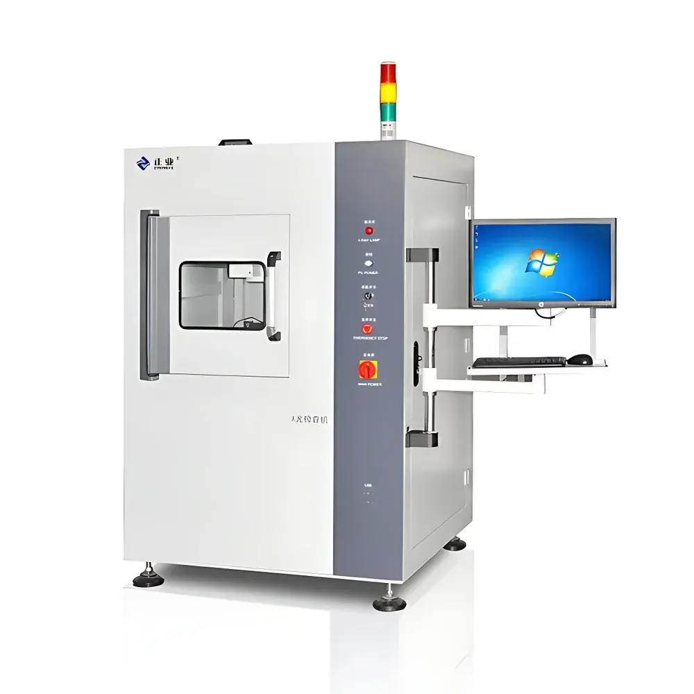
The Zhengye XG Series Semiconductor X-ray Non-destructive Inspection System is an industrial-grade microfocus X-ray imaging platform engineered for high-precision internal structural analysis of semiconductor packages, power modules, and advanced electronic assemblies. Utilizing transmission-based X-ray radiography with a sealed microfocus tube (typically operating at 90–130 kV), the system generates high-contrast, real-time digital radiographs to visualize solder joint integrity, wire bond continuity, die attach voids, lead frame misalignment, and encapsulation defects—without physical contact or sample preparation. Designed specifically for front-end and back-end semiconductor manufacturing environments, it supports inline quality assurance, failure analysis (FA), and process validation workflows in accordance with IPC-A-610, J-STD-001, and JEDEC JESD22-A111 standards.
Key Features
- Microfocus X-ray Source: Integrated air-cooled or liquid-cooled microfocus tube with focal spot size ≤5 µm, enabling sub-micron spatial resolution and sharp edge definition for fine-pitch BGA, WLP, and 3D IC package inspection.
- 2.5D Metrology Engine: Supports calibrated geometric measurements including linear distance, circle diameter, concentricity of nested circles, and point-to-center offset—traceable to NIST-certified calibration artifacts and compliant with ISO 15530-3 for coordinate metrology uncertainty estimation.
- CNC Path Programming: User-defined motion sequences (X/Y/Z/rotation) can be recorded, edited, and replayed with repeatability better than ±2 µm, facilitating rapid setup for low-volume/high-mix production lots and FA lab batch analysis.
- Intelligent Navigation Interface: Large-field-of-view live preview window with pixel-accurate mouse-driven stage control; click any region on the radiograph to trigger automated stage movement and auto-focus adjustment within <1.5 seconds.
- Digital Image Processing Suite: Real-time contrast enhancement, noise suppression (non-local means filtering), edge sharpening, and dynamic range optimization; supports DICOM, TIFF, PNG, and proprietary .XGD formats with embedded metadata (exposure time, kV/mA, magnification, timestamp).
Sample Compatibility & Compliance
The XG Series accommodates substrates up to 300 mm × 300 mm and heights up to 120 mm—including bare dies, wafer-level packages, QFNs, LGA, SiP modules, and automotive-grade power semiconductors. Sample holders are modular and vacuum-compatible for stable positioning during long-exposure tomographic scans. The system meets IEC 61000-6-3 (EMC emissions), IEC 61000-6-2 (immunity), and GB/T 18801-2015 (Chinese radiation safety standard). Optional CE marking and UL 61010-1 certification available upon configuration review. All software logs include audit trails compliant with GLP/GMP documentation requirements per FDA 21 CFR Part 11 Annex 11.
Software & Data Management
The proprietary Zhengye X-RayVision™ software provides a unified interface for acquisition, measurement, reporting, and data archiving. It features role-based user access control (administrator/operator/analyst), configurable pass/fail thresholds with statistical process control (SPC) charting (X-bar R, Cpk), and automated PDF/Excel report generation with embedded images and measurement tables. Raw image datasets and processing parameters are stored in a relational SQLite database with SHA-256 hash verification. Integration with MES systems (e.g., Siemens Opcenter, Camstar) is supported via RESTful API and OPC UA protocols for traceability across wafer fab and assembly lines.
Applications
- Solder void quantification in power module DBC substrates (IEC 60749-29)
- Wire bond lift-off and neck fracture detection in IGBT modules
- Die tilt and epoxy bleed assessment in flip-chip CSPs
- Lead frame warpage measurement pre- and post-molding (ASTM E2921)
- Void mapping in copper pillar bumps for 2.5D interposers
- Failure root cause analysis for field return units under JEDEC JESD22-A108 accelerated life testing conditions
FAQ
What is the minimum detectable defect size for solder voids in a 0.4-mm pitch QFN package?
Typical detection limit is ~25 µm diameter void under optimized kV/mA and magnification settings, validated using IPC TM-650 2.1.1.11 test coupons.
Does the system support computed tomography (CT) reconstruction?
The XG Series supports optional 360° rotational scanning hardware and third-party CT reconstruction plugins (e.g., Octopus, VGStudio Max); full CT mode requires additional mechanical stabilization and extended acquisition time.
Can measurement data be exported to SPC software such as Minitab or JMP?
Yes—CSV and XML exports include raw coordinates, tolerance bands, and statistical summaries compatible with industry-standard SPC platforms.
Is remote diagnostics and software update capability available?
Yes, via secure TLS-encrypted VNC tunnel with customer-configurable firewall rules; firmware updates follow ISO/IEC 17025 traceable version control procedures.
What training and documentation packages are provided with installation?
Includes on-site operator certification (8 hours), ISO/IEC 17025-aligned SOP templates, full technical manual (PDF + printed), and annual calibration certificate from CNAS-accredited lab.


