ZOLIX Automated Microscopy Imaging Module
| Brand | ZOLIX |
|---|---|
| Origin | Beijing, China |
| Manufacturer Type | Original Equipment Manufacturer (OEM) |
| Product Origin | Domestic (PRC) |
| Model | Automated Microscopy Imaging Module |
| Pricing | Available Upon Request |
Overview
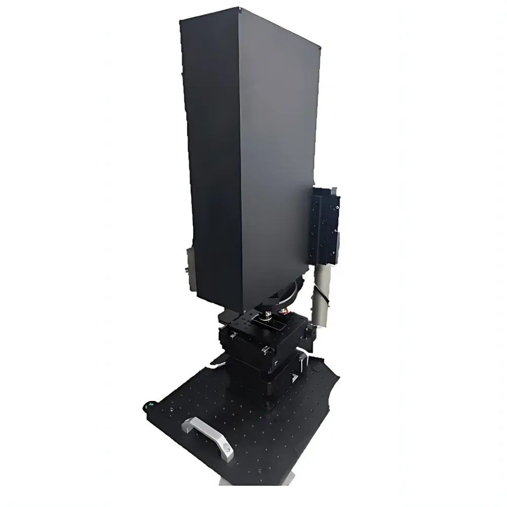
The ZOLIX Automated Microscopy Imaging Module is an industrial-grade optical imaging subsystem engineered for integration into semiconductor front-end and back-end process inspection platforms. It operates on the principle of high-precision reflected-light microscopy with real-time focus stabilization, enabling consistent, repeatable surface characterization across wafers, photomasks, and microfabricated substrates. Unlike conventional manual or semi-automated tooling microscopes, this module embeds closed-loop autofocus, programmable stage navigation, and multi-objective turret control within a compact, vibration-damped mechanical architecture—designed specifically to meet the throughput and metrology stability requirements of automated inline defect review (DR) and critical dimension (CD) measurement workflows in 200 mm and 300 mm fab environments.
Key Features
- Laser-Assisted Autofocus System: Integrates a proprietary non-contact laser displacement sensor optimized for silicon, quartz, and low-contrast bare wafer surfaces. Delivers sub-micron axial repeatability (< ±0.15 µm) without reliance on image-based contrast gradients.
- Dual-Mode Focus Strategy: Combines laser triangulation for coarse surface tracking with edge-enhanced image analysis for fine-tuning—ensuring robustness across patterned, partially patterned, and unpatterned die regions.
- Köhler Illumination Engine: A miniaturized, field-optimized Köhler illumination unit ensures uniform irradiance (>92% uniformity) across the full field-of-view, eliminating vignetting and maintaining MTF performance at both center and periphery under all magnifications.
- Full Software-Controlled Operation: Native support for industry-standard communication protocols (TCP/IP, RS-232, and USB 3.0) enables seamless integration with host inspection platforms. All functions—including objective switching, focus scanning, ROI navigation, and exposure sequencing—are scriptable via ZOLIX’s SDK (C/C++, Python, LabVIEW).
- Domestically Sourced & Controlled Supply Chain: All optomechanical components—including precision linear stages, motorized turrets, and custom-designed illumination optics—are manufactured and calibrated in ZOLIX’s ISO 9001-certified facility in Beijing, ensuring traceability and long-term service continuity.
Sample Compatibility & Compliance
The module supports standard semiconductor substrates including Si, SiC, GaN, fused silica, and sapphire wafers up to 300 mm diameter. Its optical path is compatible with dry objectives ranging from 2× to 100× (NA 0.1–0.9), accommodating both brightfield and optional darkfield configurations. The system complies with ISO 10110-7 (optical element surface quality), SEMI E10 (definition of measurement uncertainty), and meets mechanical safety requirements per GB/T 19001–2016 (equivalent to ISO 9001:2015). While not FDA-cleared, its design adheres to general principles of GLP-compliant instrumentation documentation, including audit-ready calibration logs and firmware version traceability.
Software & Data Management
The ZOLIX Imaging Control Suite provides a modular GUI for configuration, acquisition, and basic metrology annotation. For production deployment, the module exposes a comprehensive API supporting deterministic triggering, synchronized image capture with external sensors (e.g., laser scanners or AFM controllers), and metadata embedding (EXIF + custom XML tags). Raw images are saved in TIFF format with embedded spatial calibration data (pixel-to-µm mapping per objective), facilitating downstream integration with third-party metrology software such as KLA eDR, Applied Materials Discover, or open-source tools like ImageJ/Fiji with calibrated scale bars. Audit trails—including user actions, parameter changes, and timestamped calibration events—are retained locally and exportable for internal QA review.
Applications
- Automated defect localization and classification on post-lithography, post-etch, and post-CMP wafers
- Critical dimension verification of line widths, space widths, and overlay marks using calibrated edge-detection algorithms
- Mask inspection support for reticle qualification and pellicle integrity assessment
- Failure analysis (FA) workstation integration for cross-sectional imaging and bond pad inspection
- In-process monitoring of MEMS device release etch uniformity and stiction evaluation
FAQ
Is the module compatible with existing wafer handling robots and track systems?
Yes—mechanical mounting interfaces and electrical I/O follow SEMI Standard E47.1 guidelines, and motion control signals conform to GEM/SECS-II messaging protocols.
Can it be used with immersion objectives or UV illumination?
No—the current configuration is limited to dry visible-light objectives (400–700 nm); UV or NIR extensions require custom optical train redesign and are available under NRE agreement.
What is the typical focus repeatability on bare silicon wafers?
Under controlled environmental conditions (±0.5°C, <30% RH), axial repeatability is ≤ ±0.12 µm over 1,000 consecutive autofocus cycles.
Does the system support real-time image stitching or mosaic generation?
Stitching is performed offline via SDK; real-time mosaic rendering is not implemented due to computational latency constraints in inline inspection contexts.
Are calibration certificates provided with each unit?
Yes—each shipped module includes a factory calibration report traceable to NIM (National Institute of Metrology, China), covering focus sensor linearity, illumination uniformity, and pixel scale accuracy per objective.


