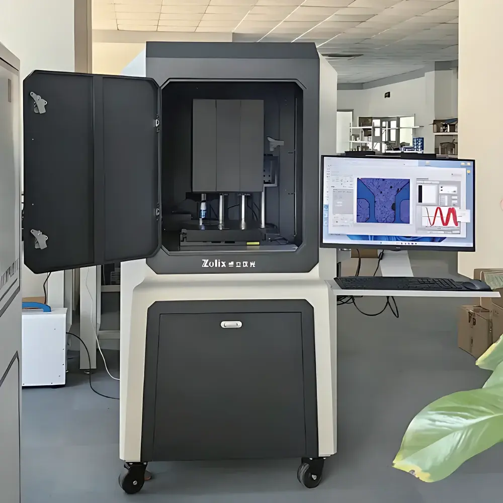
ZOLIX OminFluo990-DUV Deep-Ultraviolet Wide-Bandgap Semiconductor Photoluminescence Characterization System
| Brand | ZOLIX |
|---|---|
| Origin | Beijing, China |
| Manufacturer Type | Original Equipment Manufacturer (OEM) |
| Country of Origin | China |
| Model | OminFluo990-DUV |
| Pricing | Upon Request |
Overview
The ZOLIX OminFluo990-DUV is a purpose-built deep-ultraviolet (DUV) photoluminescence (PL) characterization system engineered for quantitative optical analysis of wide-bandgap (WBG) and ultra-wide-bandgap (UWBG) semiconductors—including AlN, AlGaN, Ga₂O₃, and diamond—within the critical 190–210 nm emission range. Unlike conventional PL systems optimized for visible or near-UV excitation, the OminFluo990-DUV integrates a custom 195 nm femtosecond pulsed laser source based on Ti:sapphire oscillator + multi-stage sum-frequency generation (SFG), enabling resonant excitation across the fundamental absorption edges of UWBG materials. Its optical architecture implements a dual-path collection scheme: a standard epi-directional (top-down) channel for 190–550 nm PL detection via high-throughput monochromator and time-correlated single-photon counting (TCSPC), and a dedicated side-collection module employing a 60°-tilted UV-grade objective to capture edge-emitted luminescence from anisotropic crystals such as AlN—where valence band inversion leads to dominant lateral photon escape. The system operates with cryogenic–high-temperature sample environments (standard: –190 °C to +600 °C; optional: 10 K–300 K), fully integrated with XYZ manual translation stages and motorized focusing for spatially resolved micro-PL mapping.
Key Features
- 195 nm deep-UV excitation source: <4 mW average power, ~100 fs pulse width, 80 MHz repetition rate, derived from Ti:sapphire oscillator (780 nm) via 2ω + SFG + SFG cascade with active group-velocity dispersion compensation
- Dual-channel spectral detection: (1) Epi-collected PL (190–550 nm) through UV-optimized microscope objective (NA ≥ 0.4, transmission >85% @ 195 nm), long-pass filtering, and Czerny–Turner monochromator; (2) Side-emitted PL (200–550 nm) via 60°-inclined UV objective and fiber-coupled input to secondary monochromator port
- Micro-scale spatial resolution: <2 µm excitation spot size at sample plane, enabled by diffraction-limited UV microscopy and active beam stabilization
- Time-resolved capability: TCSPC detection with <50 ps instrument response function (IRF), supporting multi-exponential lifetime fitting (up to 4 decay components) using deconvolution-based algorithms that self-calibrate IRF from rising edge analysis
- Modular optical rail architecture: Slot-based parallel path design allows seamless integration of Raman, photocurrent, confocal reflectance, and hyperspectral imaging modules without realignment
- In-situ laser power monitoring: Integrated pick-off beam sampling and calibrated photodiode within microscope housing enables real-time excitation intensity normalization during mapping and comparative quantification
Sample Compatibility & Compliance
The OminFluo990-DUV supports wafer-level and bulk crystal characterization of III-nitrides (AlN, AlGaN, GaN), oxides (β-Ga₂O₃, SnO₂), carbides (SiC), and emerging UWBG materials (BN, diamond). Sample mounting accommodates standard 2″–6″ wafers or diced chips on vacuum-compatible cold/furnace stages with sapphire or CaF₂ optical windows (transmission >90% @ 190–250 nm). All optical coatings, gratings, and detectors meet ISO 9001 manufacturing traceability standards. Data acquisition and storage comply with GLP/GMP-aligned metadata tagging (timestamp, temperature, laser energy, grating position, detector gain), and software export formats (HDF5, .spc, .txt) are compatible with ASTM E1317-22 spectral data exchange protocols. Optional 21 CFR Part 11-compliant audit trail and electronic signature modules are available for regulated semiconductor process development labs.
Software & Data Management
Control and analysis are unified under ZOLIX VISUALSPECTRA™ v5.x—a modular, Python-extendable platform supporting hardware abstraction layers for third-party stages, detectors, and environmental chambers. Core modules include: (i) Auto-focus-enabled PL mapping with real-time drift correction; (ii) Batch spectral processing engine applying baseline subtraction, smoothing, peak deconvolution (Gaussian/Lorentzian/Voigt), stress quantification (calibrated against Si, GaN, SiC Raman shifts), carrier concentration estimation (via PL peak broadening/shift modeling), and crystallinity assessment; (iii) TCSPC lifetime analysis with automated IRF extraction, convolution-based multi-component fitting, χ² minimization, and residual diagnostics; (iv) Multivariate analysis suite integrating PCA, hierarchical clustering, and supervised machine learning models for compositional grading and defect classification. All workflows support RECIPE scripting for unattended multi-step acquisitions and customizable GUI layouts per user role.
Applications
- Quantitative evaluation of AlN epilayer quality via near-band-edge (NBE) PL intensity ratio (205 nm / 210 nm), linewidth (<15 meV target), and lifetime (<1 ns for high-purity material)
- Strain mapping in AlGaN heterostructures using spectral shift correlation between donor-bound exciton (DBE) and NBE peaks
- Defect-related deep-level emission (DLE) identification in Ga₂O₃ across 250–450 nm, correlated with thermal treatment history
- Time-resolved carrier dynamics studies under variable temperature (10 K–600 K) to extract activation energies of non-radiative recombination centers
- Wafer-scale homogeneity assessment via 100×100 µm step-size PL intensity/lifetime mapping with <±2% repeatability over 8-hour runs
- Integration with in-line process metrology tools for closed-loop feedback in MOCVD and HVPE reactor optimization
FAQ
What is the minimum detectable PL intensity for AlN at 205 nm?
Detection limit is <500 counts/s under 195 nm excitation (1 mW, 2 µm spot), corresponding to ~10¹⁶ cm⁻³ effective donor concentration assuming known quantum efficiency.
Can the system perform simultaneous PL and Raman measurements?
Yes—via the parallel optical rail architecture; Raman excitation uses 325 nm HeCd or 532 nm DPSS laser, with spectral separation achieved using dichroic beamsplitters and independent entrance slits.
Is vacuum operation supported for air-sensitive samples?
The sample chamber accepts UHV-compatible cold stages (10⁻⁷ mbar base pressure); optional quartz viewport replacement with MgF₂ enables full DUV transmission down to 115 nm.
How is laser-induced damage avoided on fragile UWBG thin films?
Excitation fluence is actively controlled via motorized neutral density filters calibrated against NIST-traceable power meters; default mapping protocols enforce <100 µJ/cm² per pulse to prevent ablation.
Does the software support batch processing of legacy spectral datasets?
VISUALSPECTRA™ includes backward-compatible import filters for OceanInsight, Horiba, and Andor file formats, with automated unit conversion and spectral recalibration against internal Hg/Ar lamp references.


